Electron-emitting device and image-forming apparatus

a technology of electron-emitting device and image-forming apparatus, which is applied in the manufacture of electric discharge tubes/lamps, tubes with screens, discharge tubes luminescnet screens, etc., and can solve the problems of inability to make small beams, limited lifetime of fe-type devices, and inducing the thermal destruction of electron-emitting portions

Inactive Publication Date: 2004-04-06
CANON KK
View PDF5 Cites 51 Cited by
  • Summary
  • Abstract
  • Description
  • Claims
  • Application Information

AI Technical Summary

Problems solved by technology

Thermal destruction of an electron-emitting portion is induced, and the lifetime of an FE type device becomes limited, if the emission current density for causing the fluorescent material emit light is made large.
Furthermore, there is a tendency for electrons emitted from the leading edge spread out due to an electric field formed by a gate electrode, and the beam size cannot be made smaller.
This is generally performed by narrowing down an emitted electron beam by using a negative electric potential of the convergence electrode, but the manufacturing process thereof becomes complex and this invites a large increase in manufacturing costs.

Method used


Image

  • Electron-emitting device and image-forming apparatus
  • Electron-emitting device and image-forming apparatus
  • Electron-emitting device and image-forming apparatus

Examples


embodiment 1

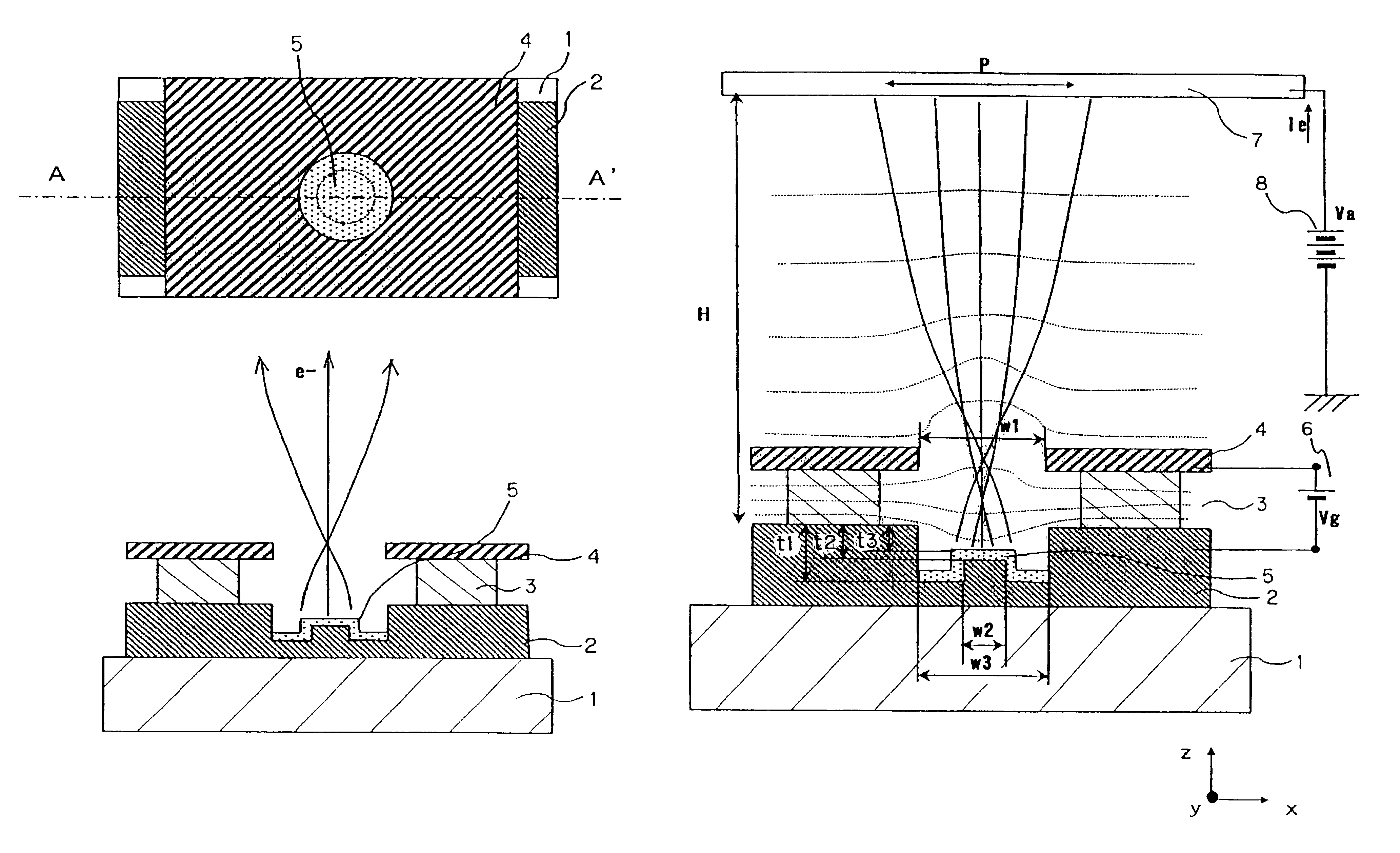
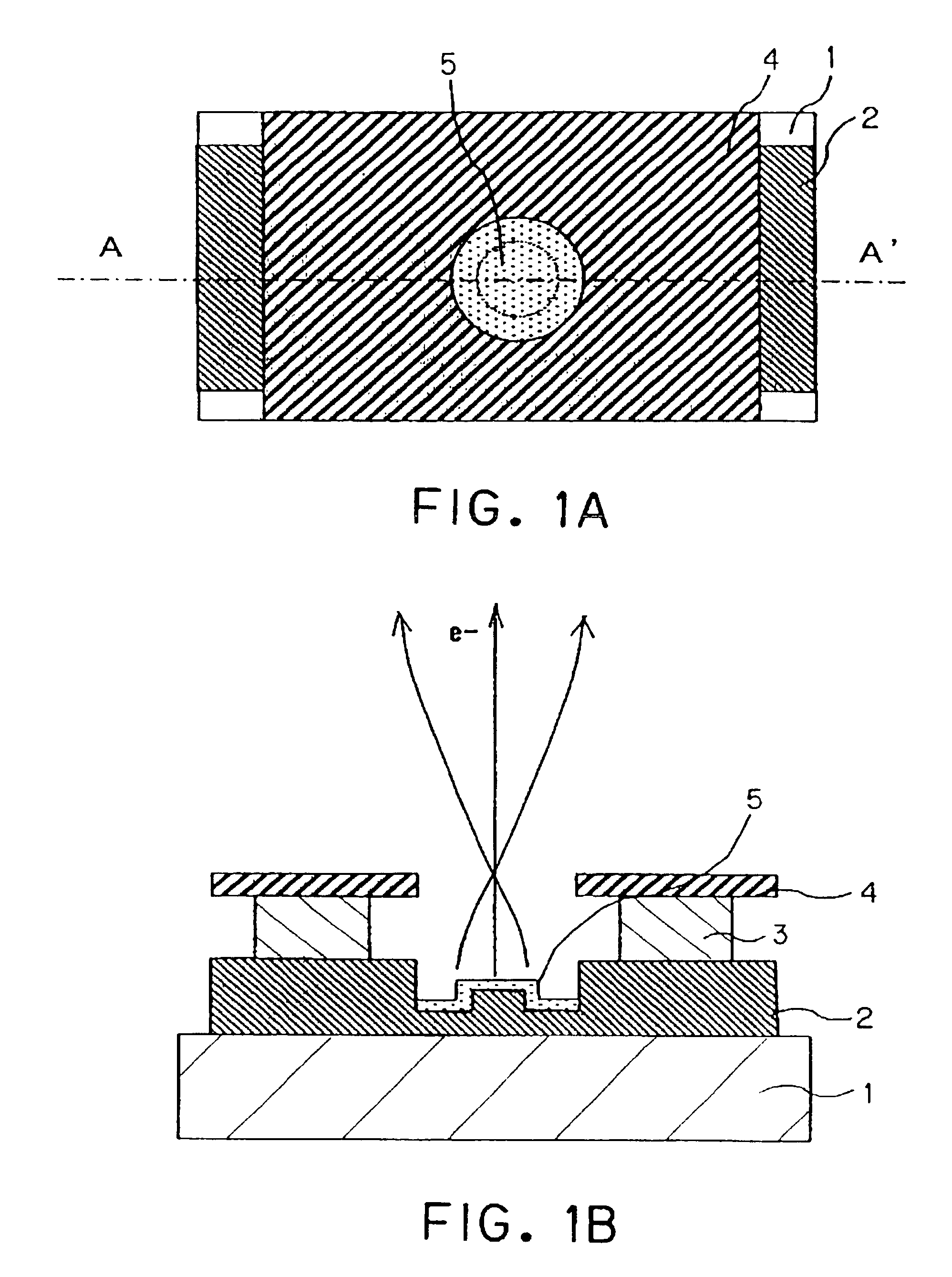
FIGS. 1A and 1B show Embodiment 1 of the present invention. Further, an example of a manufacturing method thereof is shown in FIGS. 4A to 4G. The manufacturing method is explained.

Process 1

First, soda lime glass is used as the substrate 1 as shown in FIG. 4A. Ta is formed to a thickness of 800 nm as the cathode electrode 2 after sufficient washing is performed.

Next, SiO.sub.2 is deposited to a thickness of 500 nm as the insulating layer 3, and Pt is deposited to a thickness of 100 nm as the gate electrode 4 in the stated order.

Process 2

In addition, the Al mask pattern 41 is formed as shown in FIG. 4B by utilizing photolithography.

Process 3

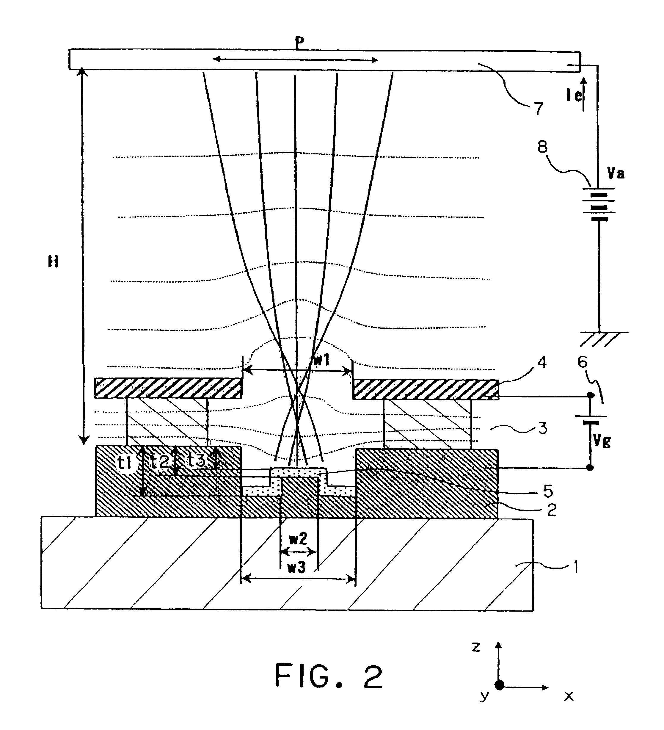
The Pt gate electrode 4 is then etched using Ar plasma etching, and the insulating layer 3 and the cathode electrode 2 are dry etched using CF.sub.4 gas, with the mask pattern 41 acting as a mask, as shown in FIG. 4C. An opening having the width w2 equal to 0.4 .mu.m, the width w3 equal to 1.2 .mu.m, and the cathode electrode 2 opening thickness t1...

embodiment 2

FIG. 10A is a variation example of Embodiment 1, and is an example in which the edge is blunt in the process of manufacturing the cathode electrode 2.

The opening is minute in Embodiment 2, and for cases in which the peripheral portion region cannot be made small compared to the opening, the above-mentioned phenomenon is caused by etching. Manufacturing is performed in Embodiment 2 with the width w3 of the opening of the gate electrode 4 being set to 0.8 .mu.m.

A beam size similar to that of Embodiment 1 can also be obtained in Embodiment 2 by optimizing t3. In this case, it is also possible to manufacture the peripheral portion and the central portion of the opening bottom face of the cathode electrode 2 by also shaving the central portion of the cathode electrode 2 when manufacturing the peripheral portion, and performing the etching process, which must be performed twice in Embodiment 1, only once here.

embodiment 3

FIG. 10B is an example in which the size w1 of the opening of the gate electrode 4 is made smaller than the opening of the cathode electrode 2. In this structure, the electron-emitting material 5 does not exist in the edge portion of the cathode electrode 2, and therefore the leak current of the electron-emitting material 5 can be reduced to nearly zero.

A method of etching by using a focused ion beam from an oblique angle can be considered in etching the peripheral portion as a manufacturing method for forming this structure.


PUM


Abstract

An electron-emitting device having a small electron beam size is proposed. In order to provide a high definition image display device having high image quality by utilizing this type of electron-emitting device and an electron source, a cathode electrode (2) has an opening which is trenched in a portion thereof, and further, the depth at which the opening is trenched is deep at a peripheral portion of the opening bottom face, and shallow at a central portion of the opening bottom face. A surface of an electron-emitting material is formed in a portion deeper than a boundary surface between the cathode electrode and an insulating layer.

Description

1. Field of the InventionThe present invention relates to an electron-emitting device, and in addition, to an image-forming apparatus which uses the electron-emitting device.2. Related Background ArtTwo types of electron-emitting devices are known conventionally: the thermoelectron source type and the cold cathode electron source type. Of these, the cold cathode electron source type refers to devices including field emission type (hereinafter referred to as the FE type) electron-emitting devices, metal / insulation layer / metal type (hereinafter referred to as the MIM type) electron-emitting devices, surface conduction type electron-emitting devices, and the like.In order to apply these types of electron-emitting devices in to an image-forming apparatus, an emission current that causes a phoshor to emit light with a sufficient luminance is necessary. Further, to obtain high definition display, electron beams to be irradiated to the fluorescent material are required to have a small diam...

Claims


Application Information

Patent Timeline
Patent Type & Authority Patents(United States)
IPC IPC(8): H01J31/12H01J1/02H01J29/04H01J1/304H01J1/00H01J1/30
CPCB82Y10/00H01J1/304H01J31/127H01J2201/30446H01J2201/30457H01J2201/30469
Inventor NISHIMURA, MICHIYO
Owner CANON KK
Why Eureka
Try Eureka