Circuit and method for implementing a write operation with TCCT-based memory cells

a memory cell and capacitively coupled technology, applied in the field of integrated circuits, can solve the problems of affecting computation processing speed, data processing rate, general limitation,

Inactive Publication Date: 2004-05-11
MICRON TECH INC +1
View PDF4 Cites 26 Cited by
  • Summary
  • Abstract
  • Description
  • Claims
  • Application Information

AI Technical Summary

Problems solved by technology

Data processing rates, however, are generally limited by the manner in which data is exchanged between the processing and memory components, and by the use of conventional memory technology.
These operations, however, can hinder computational processing speeds because processor logic is generally faster than memory access time.
That is, processing speed is generally limited by the speed at which data can be stored and retrieved from memory.
Although circuit 401 of FIG. 4 can provide for read operations, it is not well-suited to reliably support either write operations or optimized memory access operations, such as read-over-write.
In short, given the nature of TCCT-based memory cells, when an activating signal applied to a gate-like device of the thyristor, a unit of data stored previously therein can no longer be considered reliable.
Hence, the latching state of the TCCT devices in the non-targeted memory cells 1a and 3a most is likely affected, thus making the previously stored data bits from these cells no longer reliable.
Consequently, simple open-bit line architectures that have been used with conventional memory technologies are not well-suited to reliably support write operations and read-over-write operations for arrays including TCCT-based memory cells.

Method used


Image

  • Circuit and method for implementing a write operation with TCCT-based memory cells
  • Circuit and method for implementing a write operation with TCCT-based memory cells
  • Circuit and method for implementing a write operation with TCCT-based memory cells

Examples


Embodiment Construction

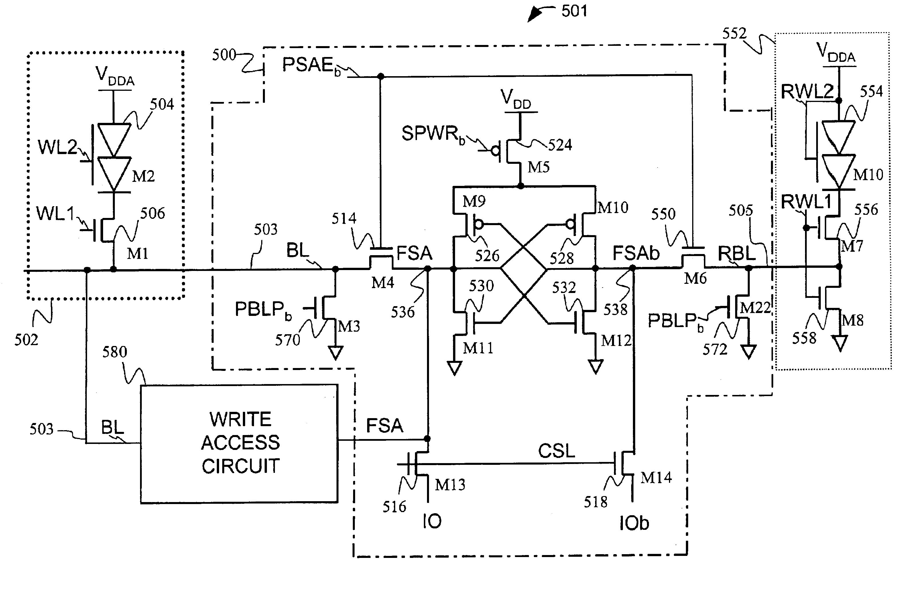
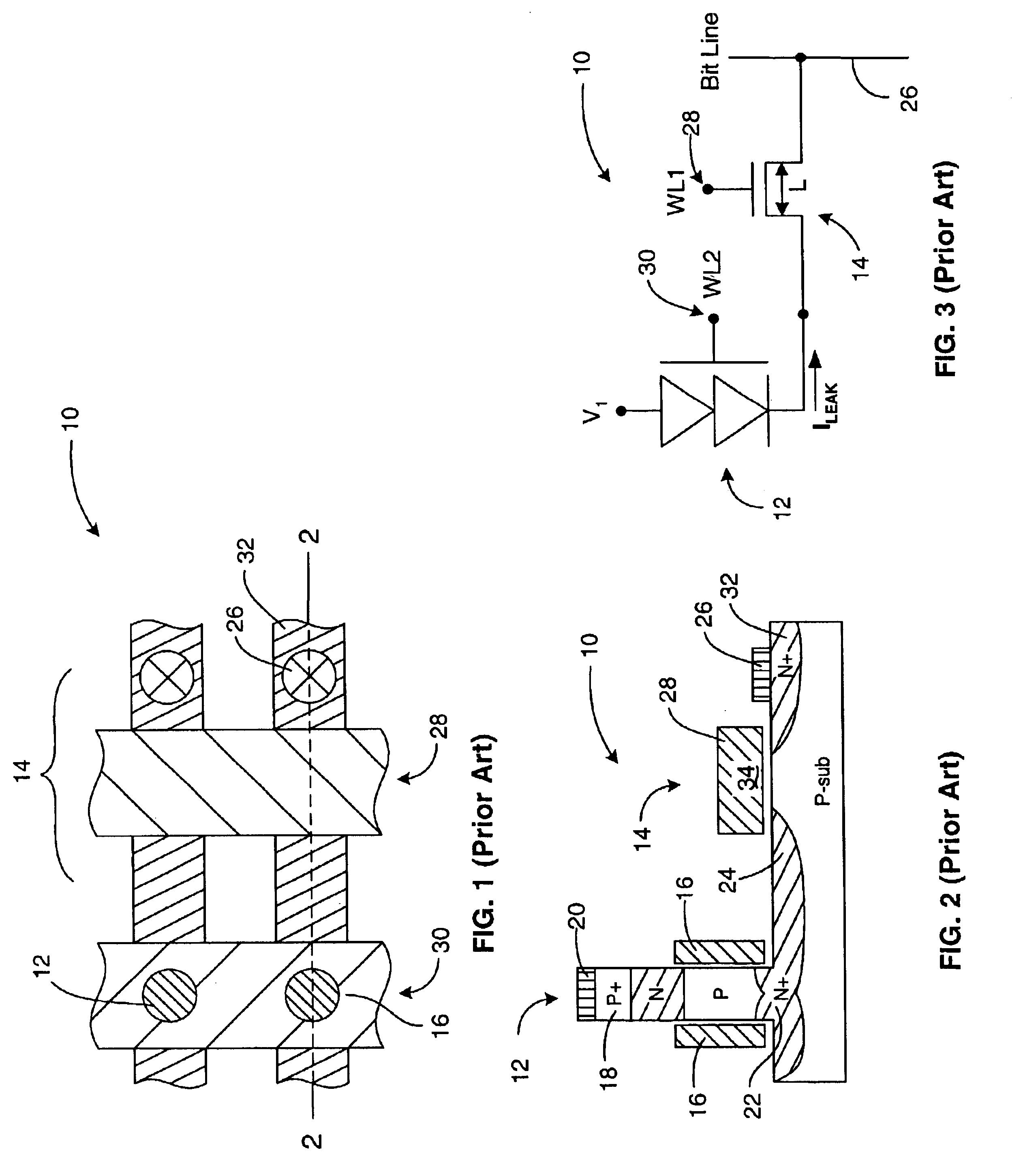
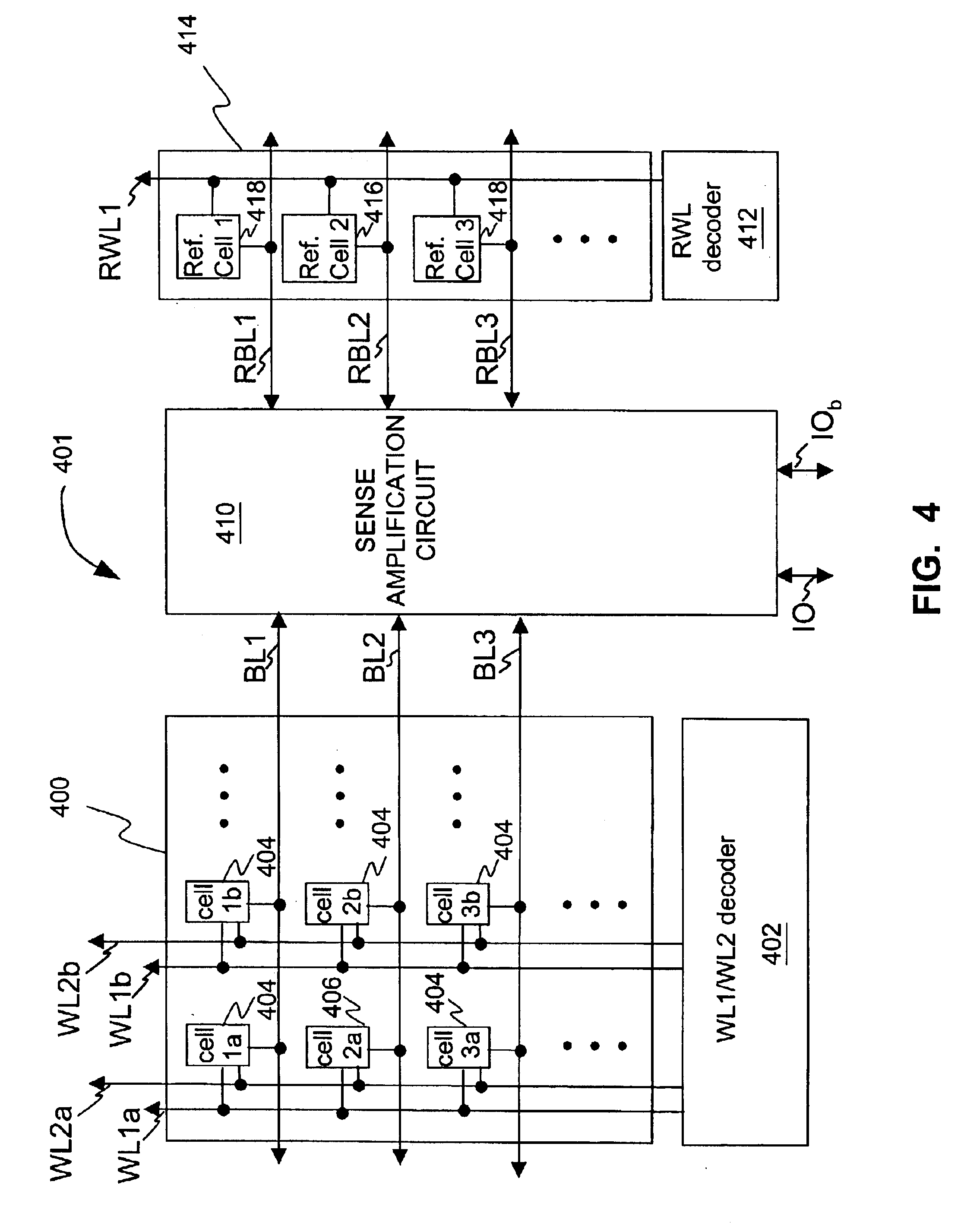
Detailed descriptions of exemplary embodiments are provided herein. It is to be understood, however, that the present invention may be embodied in various forms. Therefore, specific details disclosed herein are not to be interpreted as limiting, but rather as a basis for the claims and as a representative basis for teaching one skilled in the art to employ the present invention in virtually any appropriately detailed system, structure, method, process or manner.

The term "device" is used herein to describe both a discrete semiconductor circuit element, such as a MOS transistor or a TCCT device, as well as a semiconductor product. A memory semiconductor product can be referred also as a memory "chip" or "integrated circuit" and is a circuit element operating cooperatively with other semiconductor products, such as a microprocessor. An "operation" described herein can refer to a process, from a request to initiate. the process to the completion of the process, such as reading data from...


PUM


Abstract

The present invention provides a circuit and a method for providing nondestructive write operations and optimized memory access operations with reduced power consumption during memory access, such as during write operations. In one embodiment, a memory device comprises a memory cell configured to store a first data bit. The memory device also comprises a write access circuit coupled to the memory cell for providing a write data bit having a write data bit magnitude. The write access circuit is configured to adjust the write data bit magnitude to an intermediate logic state magnitude in a memory operation.

Description

1. Field of the InventionThe present invention relates generally to integrated circuits, and in particular, to a circuit and a method for performing write operations with thinly capacitively-coupled thyristor ("TCCT")-based memory cells.2. Description of Related ArtThe rate at which data must be processed is ever increasing in computing-related applications. For example, burgeoning computer graphic applications require faster execution of underlying computational processes to render enhanced three-dimensional images, especially when motion is added. As another example, data network applications demand enhanced computational processes in routing increasing amounts of data (using network elements, such as routers) over decreasing amounts of network bandwidth. The rate at which underlying computational processes are executed depends on the combined functionality of a main processing component, such as a central processing unit ("CPU") and / or a peripheral device (e.g., graphics processo...

Claims


Application Information

Patent Timeline
Patent Type & Authority Patents(United States)
IPC IPC(8): G11C11/39
CPCG11C11/39
Inventor YOON, SEI-SEUNGJUNG, SEONG-OOK
Owner MICRON TECH INC
Why Eureka
Try Eureka