

Feedback method utilizing lithographic exposure field dimensions to predict process tool overlay settings
a lithographic exposure field and overlay setting technology, applied in the direction of adaptive control, semiconductor/solid-state device testing/measurement, instruments, etc., can solve the problem of not being able to lithographically transfer ("print") all structures simultaneously across the full wafer
- Summary
- Abstract
- Description
- Claims
- Application Information
AI Technical Summary
Benefits of technology
Problems solved by technology
Method used
Image

Examples
Embodiment Construction
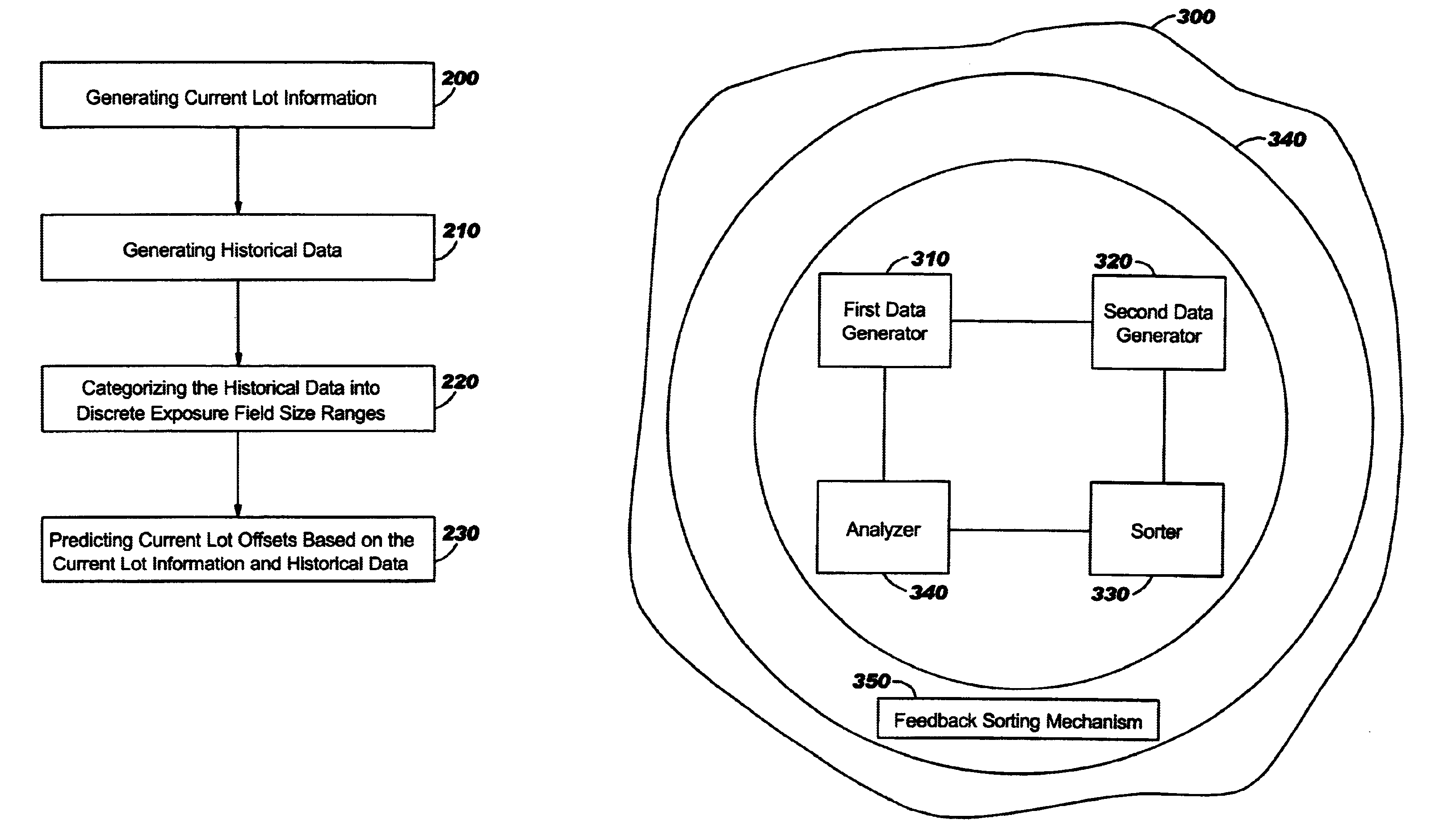
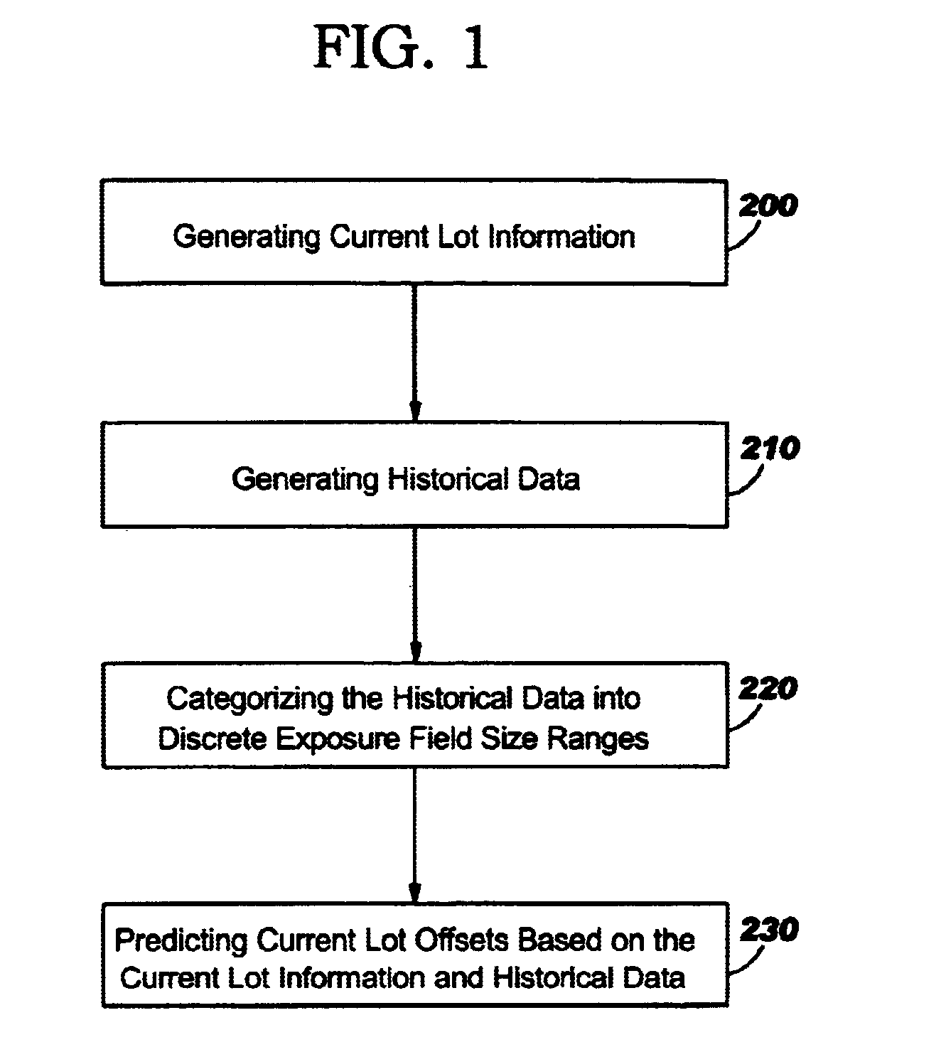
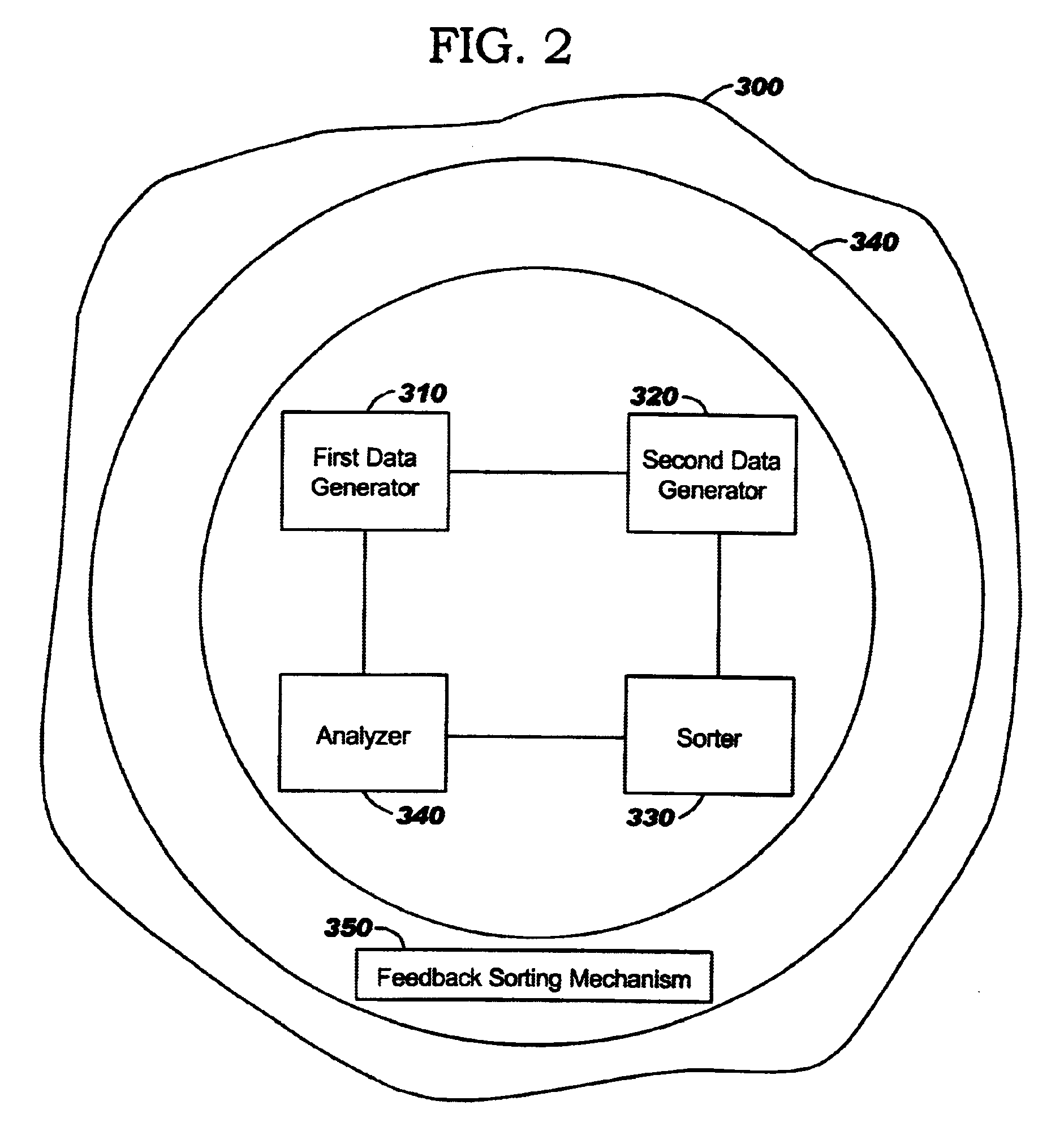
As mentioned, there remains a need for a new feedback sorting criteria to substantially increase the likelihood of achieving overlay specifications for the first pass through the lithographic tool at each lithographic process operation. According to the present invention, additional sorting criteria is used in the overlay monitoring process, specifically lithographic exposure field size, in order to increase the likelihood of meeting overlay specifications on the first pass through the lithographic process tool, especially for first time use reticles, as well as Manufacturing WIP (Work-In-Progress) Profiles comprising many unique parts, each at low volumes. Referring now to the drawings, and more particularly to FIGS. 1 through 8, there are shown preferred embodiments of the method and structures according to the present invention.
The present invention includes a method for predicting process tool overlay settings based on the lithographic field size of the current lot. A method of ...
PUM
| Property | Measurement | Unit |
|---|---|---|
| diameter | aaaaa | aaaaa |
| size | aaaaa | aaaaa |
| exposure wavelengths | aaaaa | aaaaa |
Abstract
Description
Claims
Application Information