Electroluminescent devices containing thermal protective layers

a technology of electroluminescent devices and protective layers, which is applied in the direction of discharge tubes/lamp details, discharge tubes luminescnet screens, electric discharge lamps, etc., can solve the problems of poor thermal stability, unsuitability of el devices, and non-functionality of organic el devices, so as to improve the thermal stability of the device, increase the resistance of the device to shorting, and improve the effect of stability

Inactive Publication Date: 2004-07-20
LG DISPLAY CO LTD
View PDF29 Cites 54 Cited by
  • Summary
  • Abstract
  • Description
  • Claims
  • Application Information

AI Technical Summary

Benefits of technology

The present invention in embodiments overcomes or minimizes the above disadvantages of a number of known organic EL devices, which disadvantages primarily relate to device shorting at high temperatures, and which embodiments provide organic EL devices with enhanced stability at these temperatures. High temperature refers, for example, to above 60.degree. C., and specifically in the range of about 70.degree. C. to about 100.degree. C., or higher, such as, for example 120.degree. C. The present invention also embodies an organic EL device that contains at least one thermal protective element, for example up to four elements, and preferably one or two, wherein the thermal protective element is comprised of a single layer or a plurality of stacked layers laminated in contact to each other, and typically up to three layers. The thermal protective element(s) can be laminated in between or on top the other components (layers) of the organic light emitting device. The thermal protective element(s), for example, increase(s) the device resistance to shorting at elevated temperatures, and thus improves the thermal stability thereof.

Problems solved by technology

A problem common to this type of known organic EL devices is poor thermal stability which usually renders the EL device unsuitable for technological applications that require high durability of devices at high temperatures, and which temperatures are, for example, above about 60.degree. C., and specifically, temperatures in the range of about 70.degree. C. to about 100.degree. C.
At these high temperatures, device shorting often occurs leading to high leakage currents, thus rendering the organic EL devices nonfunctional (reference, for example, Zhou et al., "Real-time observation of temperature rise and thermal breakdown processes in organic LEDs using an IR imaging and analysis system", Advanced Materials 12, pp 265-269, 2000).
However, these devices are believed to require excitation voltages on the order of 100 volts or greater.
However, as described in the S. Naka et al. article, these single mixed layer organic light emitting devices are generally less efficient than multi-layer organic light emitting devices.
Recent EL research results indicate that those devices including only a single mixed layer of a hole transport material (composed of NBP, a naphthyl-substituted benzidine derivative) and an emitting electron transport material (composed of Alq.sub.3, tris(8-hydroxyquinoline) aluminum) are inherently believed to be unstable.
The instability of these devices is believed to be caused by the direct contact between the electron transport material in the mixed layer and the hole injecting contact comprised of indium tin oxide (ITO), which results in the formation of the unstable cationic electronic transport material, and the instability of the mixed layer / cathode interface, see, H. Aziz et al., Science 283, 1900 (1999), the disclosure of which is totally incorporated herein by reference in its entirety.
However, such known devices have been found to be generally less efficient than conventional devices including separate layers of hole transport material and emitting electron transport material.
While recent progress in organic EL research has perhaps elevated the potential of organic EL devices, the operational stability of current available devices may still be below expectations.
A number of known organic light emitting devices have relatively short operational lifetimes before their luminance drops to some percentage of its initial value.
Moreover, at these high temperatures, the susceptibility of the organic light emitting devices is increased as described, for example, in Zhou et al., "Real-time observation of temperature rise and thermal breakdown processes in organic LEDs using an IR imaging and analysis system", Advanced Materials 12, pp 265-269, 2000, which further reduces the stability of the devices.

Method used


Image

  • Electroluminescent devices containing thermal protective layers
  • Electroluminescent devices containing thermal protective layers
  • Electroluminescent devices containing thermal protective layers

Examples


examples

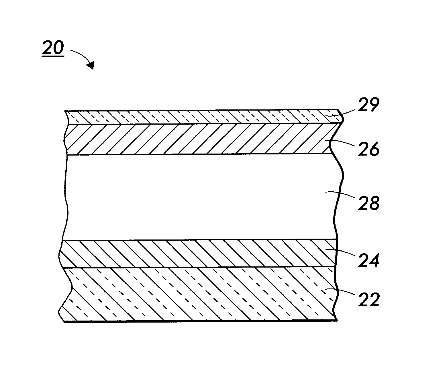
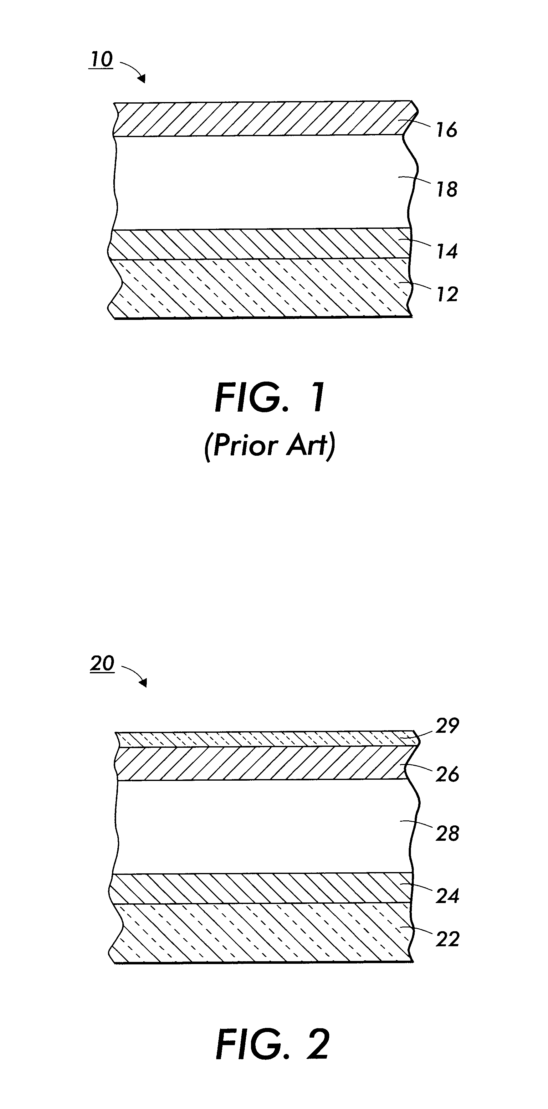
A first organic light emitting device according to this invention having a structure, such as device 20 shown in FIG. 2, was formed and evaluated. In this device a naphthyl-substituted benzedrine derivative, N,N'-di-1-naphthyl-N,N'-diphenyl-1,1'-biphenyl-1,1'-biphenyl-4,4'-diamine (NPB), and tris(8-hydroxyquinoline) aluminum (Alq.sub.3), was used as the hole transport material and the electron transport material, respectively, comprising the light emitting region 28. The light emitting region 28 was comprised of (i) a hole transport region of about 80 nanometers thick comprised of NPB, (ii) a mixed region of about 80 nanometers thick comprised of about 49.9 weight percent of NPB, about 49.9 weight percent of AlQ.sub.3, and about 0.2 weight percent of dimethylethylquinacridone (DMQ) emitting dopant, and (iii) an electron transport region of about 20 nanometers thick comprised of AlQ.sub.3. The light emitting region 28 was interposed or situated in between the anode 24 comprised of in...


PUM


Abstract

The disclosure provided relates to an organic light emitting device containinga substrate;a first electrode;a light emitting region comprising an organic luminescent material;a second electrode, and a protective thermal layer or thermal layers, and which layer is contained on the first electrode, the second electrode, the first and second electrode, and / or is contained on other layers in the device.

Description

COPENDING APPLICATIONSIllustrated in copending applications U.S. Ser. No. 09 / 770,159, filed concurrently herewith, the disclosure of which is totally incorporated herein by reference, is an organic light emitting device, comprising in an optional sequence(i) a substrate;(ii) a first electrode;(iii) a mixed region comprising a mixture of a hole transport material and an electron transport material, and wherein this mixed region includes at least one organic luminescent material;(iv) a second electrode;(v) a thermal protective element coated on the second electrode; wherein one of the two said electrodes is a hole injection anode, and one of the two said electrodes is an electron injection cathode, and wherein the organic light emitting device further comprises;(vi) a hole transport region, interposed between the anode and the mixed region, wherein the hole transport region optionally includes a buffer layer; and(vii) an electron transport region interposed between the second electrod...

Claims


Application Information

Patent Timeline
Patent Type & Authority Patents(United States)
IPC IPC(8): H01L51/50H01L51/52
CPCH01L51/5237H10K50/844
Inventor AZIZ, HANYPOPOVIC, ZORAN D.HU, NAN-XING
Owner LG DISPLAY CO LTD
Why Eureka
Try Eureka