Passivating inorganic bottom anti-reflective coating (BARC) using rapid thermal anneal (RTA) with oxidizing gas

a technology of anti-reflective coating and inorganic bottom, which is applied in the direction of semiconductor devices, photomechanical devices, instruments, etc., can solve the problems of reducing the overall cost per transistor, the ability to form and pattern components such as gate conductors and gate dielectrics on such reduced scales, consistently, robustly and reproducibly, and the effect of increasing the density and number

Inactive Publication Date: 2004-09-21
GLOBALFOUNDRIES INC
View PDF2 Cites 32 Cited by
  • Summary
  • Abstract
  • Description
  • Claims
  • Application Information

AI Technical Summary

Problems solved by technology

Additionally, reducing the size, or scale, of the components of a typical transistor also increases the density, and number, of the transistors that can be produced on a given amount of wafer real estate, lowering the overall cost per transistor as well as the cost of integrated circuit devices incorporating such transistors.
The ability to form and pattern components such as the gate conductor and gate dielectric on such reduced scales, consistently, robustly and reproducibly, is limited by, among other things, physical limits imposed by photolithography.
However, residual nitrides at the surface of an inorganic bottom anti-reflective coating (BARC) typically used in deep ultraviolet (DUV) photolithography may cause "footing" or neutralization of the Photo Acid Generator (PAG) in deep ultraviolet (DUV) photoresists at the interface between the inorganic bottom anti-reflective coating (BARC) and an overlying deep ultraviolet (DUV) photoresist layer.
Footing may lead to deep ultraviolet (DUV) photolithography reworks, increasing manufacturing costs and decreasing throughput.
However, this approach is often not effective at passivating the residual nitrides at the surface of the inorganic bottom anti-reflective coatings (BARCs).
However, this approach is often not stable, and, therefore is also often not effective at passivating the residual nitrides at the surface of the inorganic bottom anti-reflective coatings (BARCs).

Method used


Image

  • Passivating inorganic bottom anti-reflective coating (BARC) using rapid thermal anneal (RTA) with oxidizing gas
  • Passivating inorganic bottom anti-reflective coating (BARC) using rapid thermal anneal (RTA) with oxidizing gas
  • Passivating inorganic bottom anti-reflective coating (BARC) using rapid thermal anneal (RTA) with oxidizing gas

Examples


Embodiment Construction

Illustrative embodiments of the invention are described below. In the interest of clarity, not all features of an actual implementation are described in this specification. It will of course be appreciated that in the development of any such actual embodiment, numerous implementation-specific decisions must be made to achieve the developers' specific goals, such as compliance with system-related and business-related constraints, which will vary from one implementation to another. Moreover, it will be appreciated that such a development effort might be complex and time-consuming, but would nevertheless be a routine undertaking for those of ordinary skill in the art having the benefit of this disclosure.

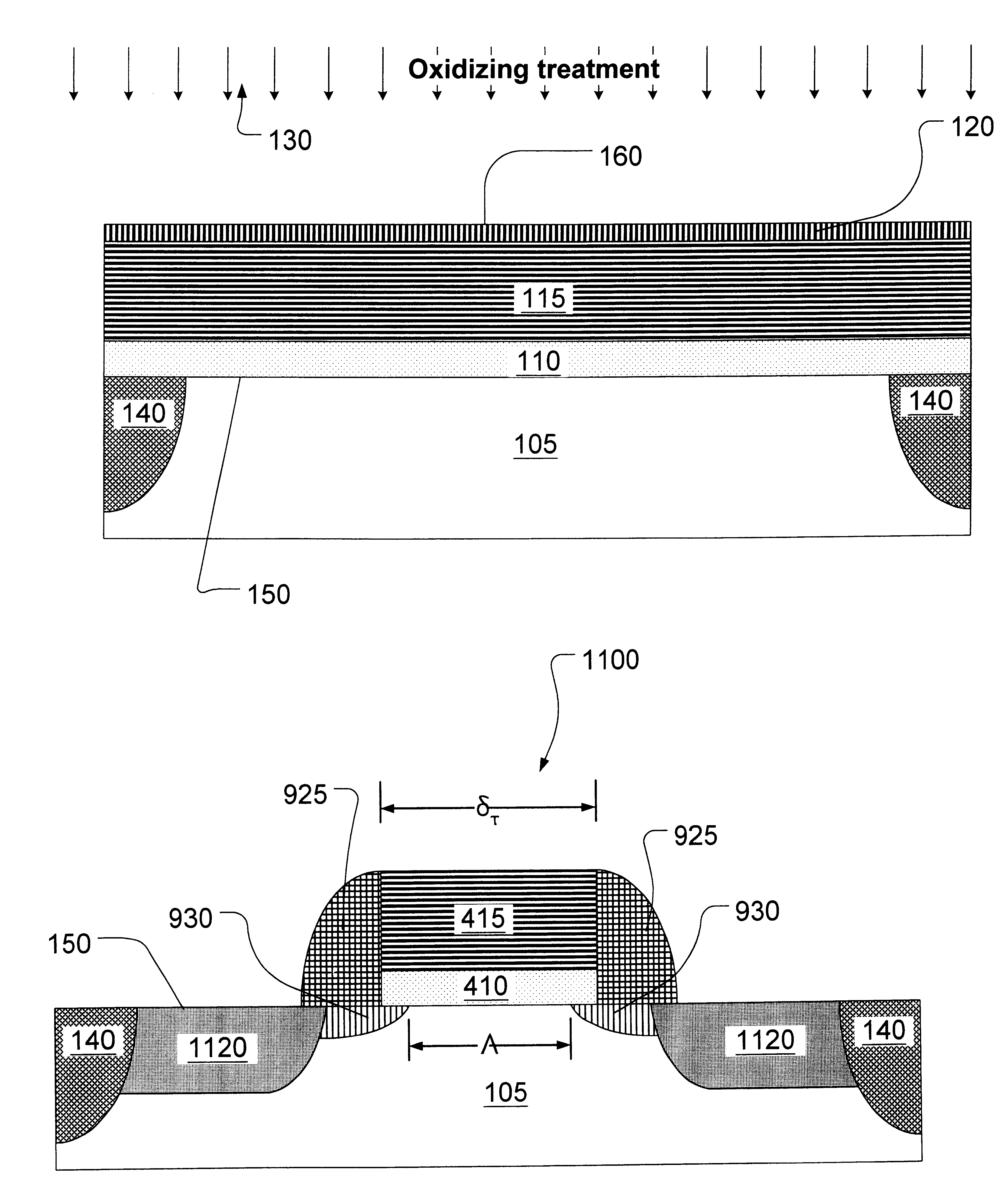
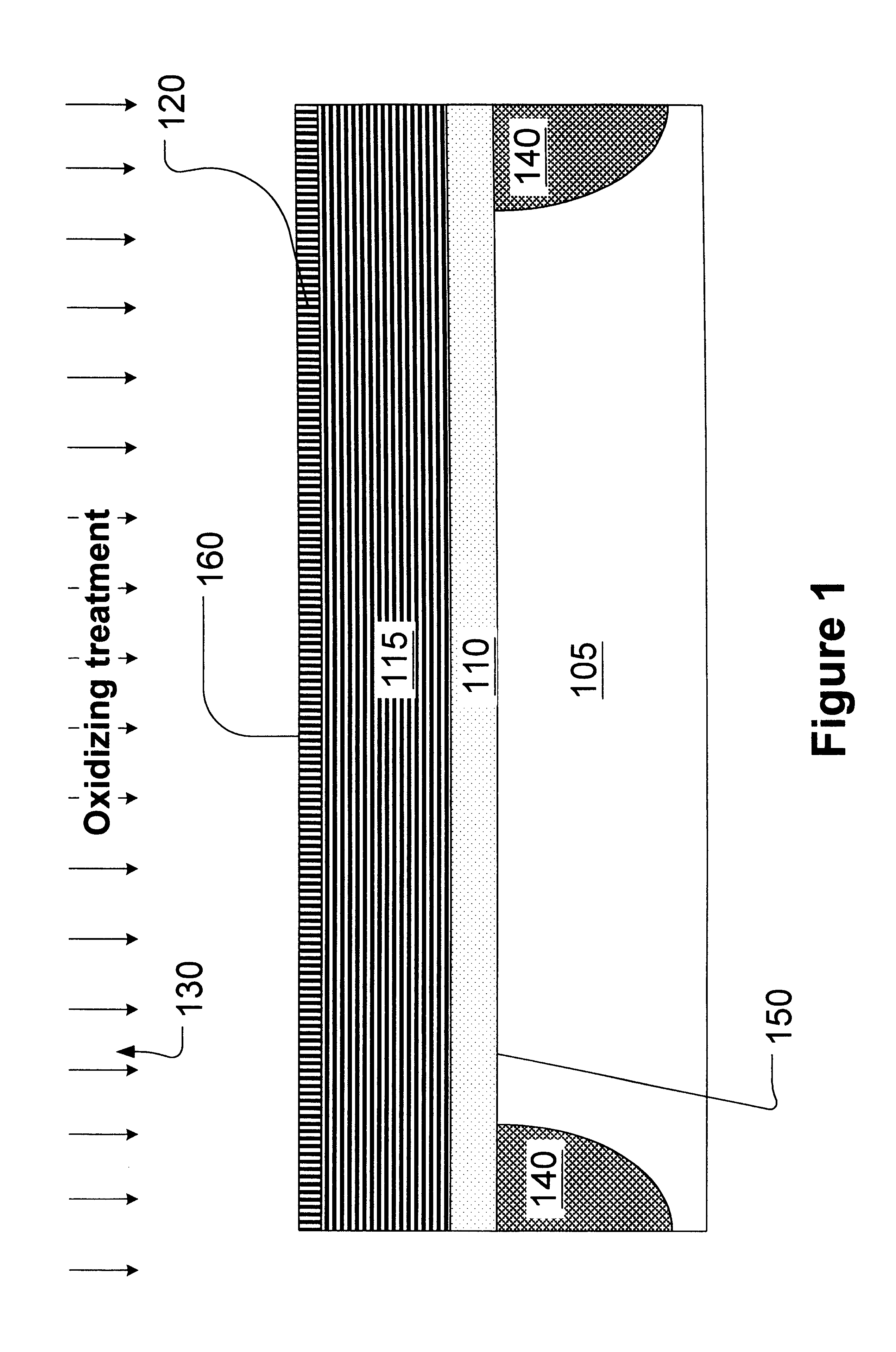
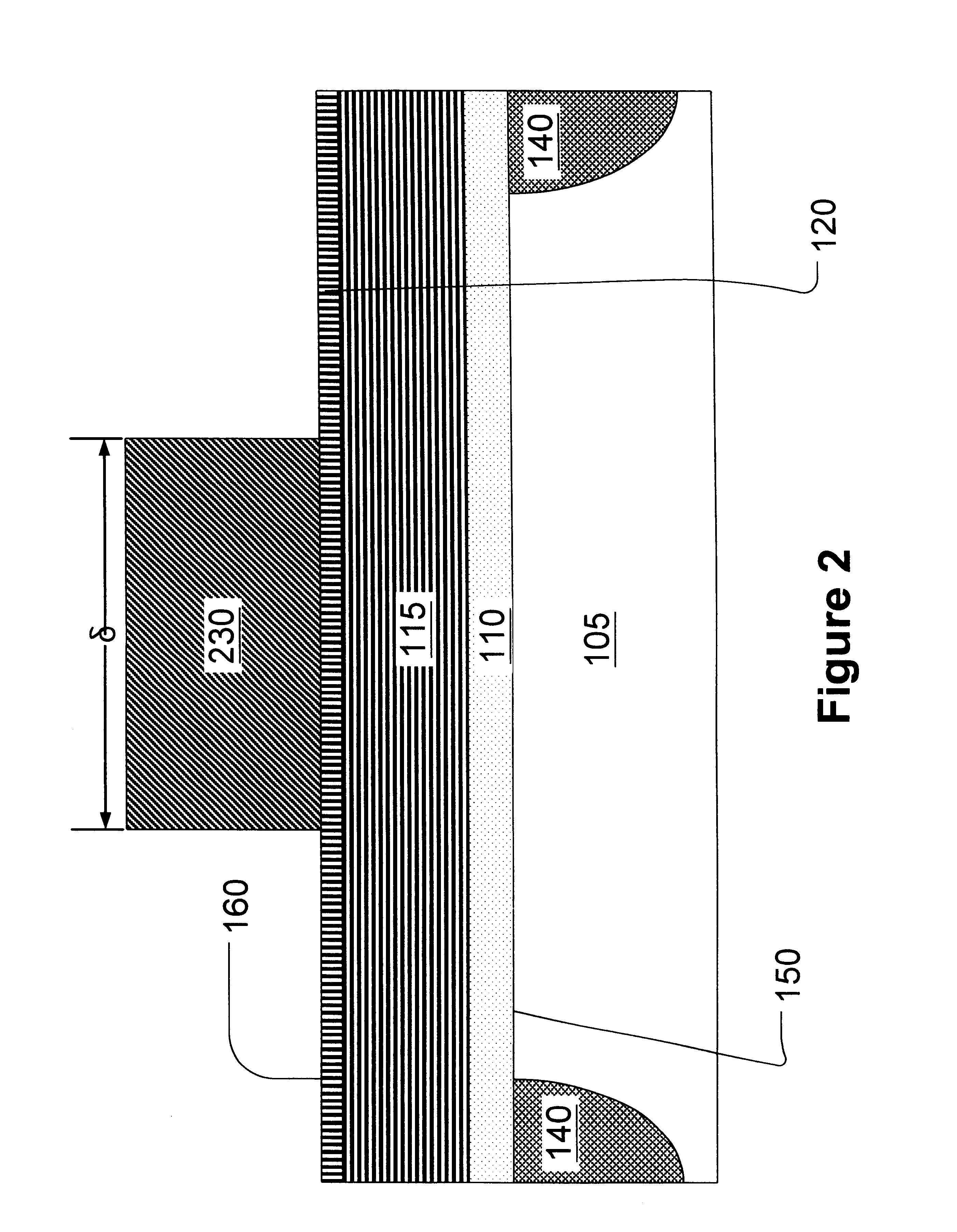
Illustrative embodiments of a method for semiconductor device fabrication according to the present invention are shown in FIGS. 1-11. Although the various regions and structures of a semiconductor device are depicted in the drawings as having very precise, sharp configurations and prof...


PUM

PropertyMeasurementUnit
dielectric constantaaaaaaaaaa
equivalent oxide thicknessaaaaaaaaaa
thicknessaaaaaaaaaa

Abstract

A method is provided, the method including forming a gate dielectric layer above a substrate layer and forming a gate conductor layer above the gate dielectric layer. The method also includes forming an inorganic bottom anti-reflective coating layer above the gate conductor layer and treating the inorganic bottom anti-reflective coating layer with an oxidizing treatment during a rapid thermal anneal process.

Description

1. Field of the InventionThis invention relates generally to semiconductor fabrication technology, and, more particularly, to techniques for manufacturing semiconductor devices with reduced critical dimensions.2. Description of the Related ArtThere is a constant drive within the semiconductor industry to increase the operating speed of integrated circuit devices, e.g., microprocessors, memory devices, and the like. This drive is fueled by consumer demands for computers and electronic devices that operate at increasingly greater speeds. This demand for increased speed has resulted in a continual reduction in the size of semiconductor devices, e.g., transistors. That is, many components of a typical field effect transistor (FET), e.g., channel length, junction depths, gate dielectric thickness, and the like, are reduced. All other things being equal, the smaller the channel length of the FET, the faster the transistor will operate. Thus, there is a constant drive to reduce the size, o...

Claims


Application Information

Patent Timeline
Patent Type & Authority Patents(United States)
IPC IPC(8): H01L21/027H01L21/28H01L21/02G03F7/09H01L29/423H01L21/3065H01L21/318H01L29/49H01L29/78
CPCH01L21/0276H01L21/28123G03F7/091Y10S438/958Y10S438/952H01L21/027
Inventor STEPHEN, ALAN D.EXTERKAMP, MICHAEL E.DOAN, JONATHAN
Owner GLOBALFOUNDRIES INC
Why Eureka
Try Eureka