Method, sensing device and optical pointing device including a sensing device for comparing light intensity between pixels

a sensing device and light intensity technology, applied in the field of pointing devices, can solve the problems of specific circuitry, increase the power consumption and complexity of the sensing device, reduce the available die area, etc., and achieve the reduction of noise sensitivity, power consumption and complexity, and the effect of die area

Inactive Publication Date: 2004-10-19
EM MICROELECTRONIC-MARIN
View PDF4 Cites 25 Cited by
  • Summary
  • Abstract
  • Description
  • Claims
  • Application Information

AI Technical Summary

Benefits of technology

According to the present invention, a time-based scaling scheme is implemented thereby allowing the scaling circuits of the prior art to be eliminated. As a consequence, die area as well as power consumption and complexity is reduced. In addition, the scaling factor may simply be adjusted by changing the ratio between the first time period and second time period (also referred to as integration period). Furthermore, this time-based scaling scheme may easily be adapted to implement a hysteresis function that allows sensitivity to noise to be reduced.
Level detection means may be provided for detecting when a first one of the integrated signals generated by the pixel integrating circuits reaches at least first and second determined levels. Accordingly, the first and second time periods are defined by the time for the first one of the integrated signals to reaches these first and second levels. In this case, this time-based scaling scheme also allows time-division to be used to separate analog and digital circuit operations, and in particular inhibit the clock signal supplied to processing means of the optical pointing device. This clock signal inhibition during analog measurement (i.e. during the integration period) eliminates digital impact (coupling, noise) to analog operations, thereby minimizing analog circuit errors and maximizing system sensitivity.
Last but not least, the above solution allows to maximise contrast over the area of the die since the integrating circuits will run until the integrated signal of the brightest pixel of the photodetector array reaches the maximum integration level. The integration time will therefore be dependent on the illumination level, and contrast, for a given illumination level, is always maximized.
Contrast ratio sensing may also easily be implemented by testing all pixels, upon the end of integration, via an analog circuit to detect the minimum integration level. This provides a measurement of the actual signal contrast seen by the sensor array.

Problems solved by technology

One serious disadvantage of the two examples illustrated in FIGS. 1 and 2 resides in the fact that they both require specific circuitry for generating the scaled image of the signal outputted by the photosensitive elements.
This circuitry thus reduces the available die area and increases the power consumption and complexity of the sensing device.
An additional disadvantage of the above two examples resides in the fact that one has very little control on the scaling factor K of the circuit.
Once this scaling factor is defined during fabrication by an adequate choice of the dimensions of the corresponding electronic components, this scaling factor cannot be adjusted by the user.
According to the prior art solution, one would again have little control and adjustment capability of this hysteresis function.

Method used


Image

  • Method, sensing device and optical pointing device including a sensing device for comparing light intensity between pixels
  • Method, sensing device and optical pointing device including a sensing device for comparing light intensity between pixels
  • Method, sensing device and optical pointing device including a sensing device for comparing light intensity between pixels

Examples


Embodiment Construction

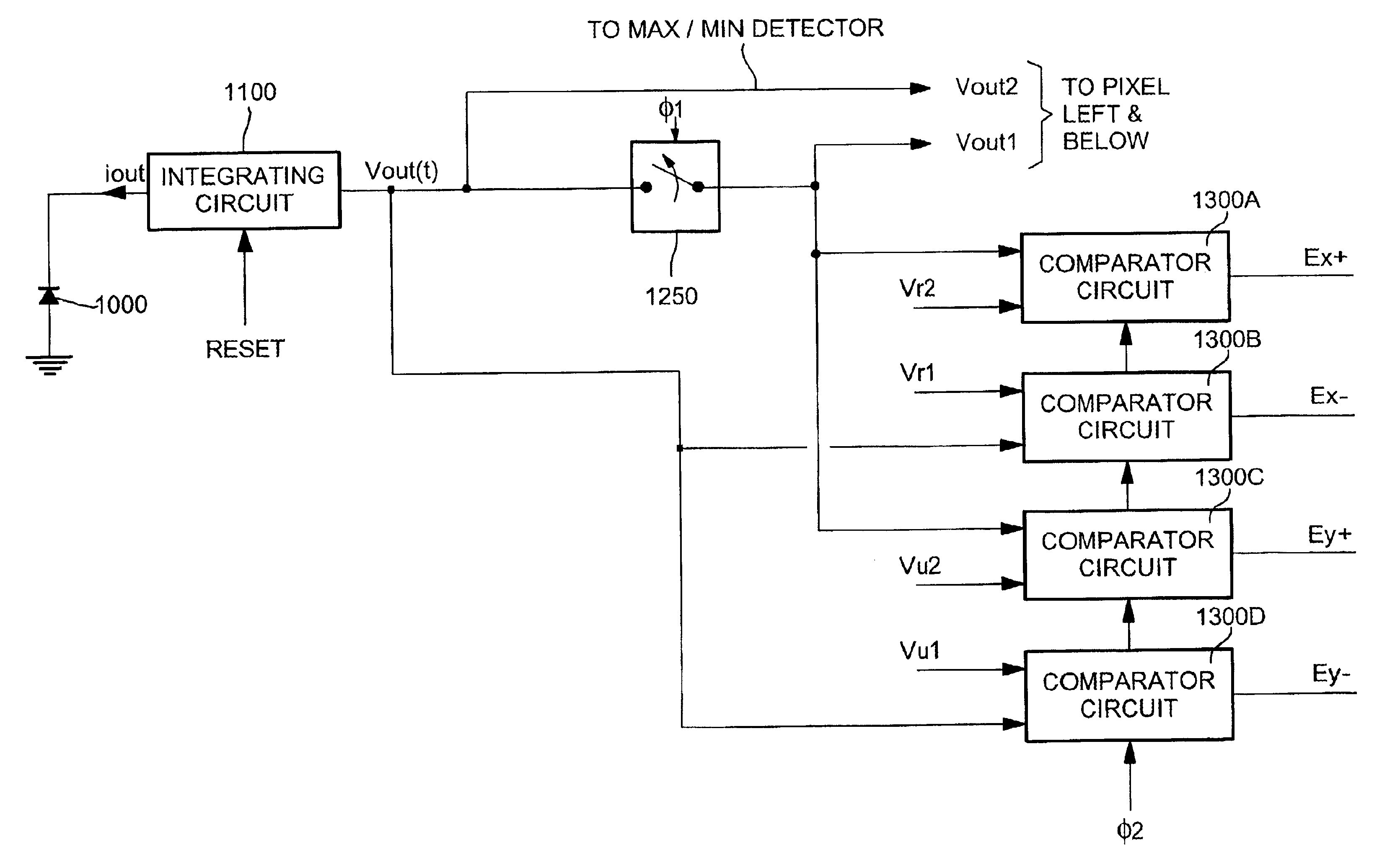
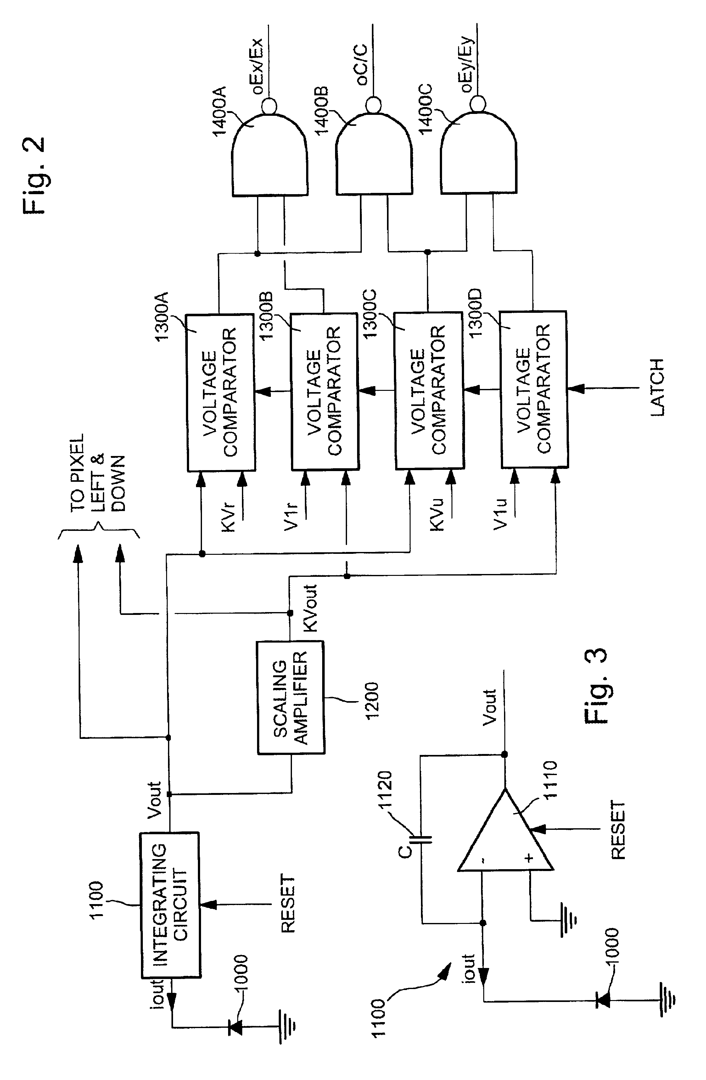
FIG. 4 is a generalized schematic bloc diagram of an optical pointing device in accordance with the present invention. It comprises a photodetector array 420 including a plurality of pixels, this photodetector array 420 being connected to processing means 400 which consists, in a non limiting manner, of a micro-controller, microprocessor or other adequate logic circuitry for processing the signals outputted by the photodetector array 420. As schematically illustrated in FIG. 5, the photodetector array 420 is for instance a regular array, preferably square, having M pixel rows (parallel to axis x) and N pixel columns (parallel to axis y). A typical configuration is for instance a 15.times.15 pixels array. Each pixel of the photodetector array 420, designated by reference numeral 4000, essentially includes a photosensitive area 1000 forming a photodiode (or alternatively a phototransistor) and active circuitry 4500 including preamplifier means and comparator circuits for determining e...


PUM


Abstract

There is described a method, a sensing device as well as an optical pointing device including a sensing device for comparing light intensity between pixels. Light intensity between pairs of pixels of a photodetector array is compared as follows. First and second output signals generated by the photosensitive elements of a first and a second pixel of each pair are integrated over time to respectively provide first and second integrated signals. Integration of the first output signal is interrupted at the end of a first time period and the resulting first integrated signal is stored. Integration of the second output signal is continued until the end of a second time period and the resulting second integrated signal is compared to the stored first integrated signal to provide an output signal representative of an edge condition between the first and second pixel.

Description

FIELD OF THE INVENTIONThe present invention generally relates to pointing devices, in particular for controlling the position of a cursor on a screen, such as the display of a personal computer, workstation or other computing devices having a graphic user interface. Such pointing devices may for instance include mice, trackballs and other computer peripherals for controlling the position of a cursor on a display screen.The present invention more particularly relates to the field of optical pointing devices which comprise an optical sensing device including a photodetector array for measuring the varying intensity pattern of a portion of a surface which is illuminated with radiation and for extracting information about the relative motion between the photodetector array and the illuminated portion of the surface.BACKGROUND OF THE INVENTIONOptical pointing devices are already known in the art. U.S. Pat. No. 5,288,993, which is incorporated herein by reference, for instance discloses a...

Claims


Application Information

Patent Timeline
Patent Type & Authority Patents(United States)
IPC IPC(8): G06M7/00H01J40/00H01J40/14
CPCG06F3/0317
Inventor ROTZOLL, ROBERT R.BUESCHER, KEVIN SCOTTLAUFFENBURGER, JAMES HAROLD
Owner EM MICROELECTRONIC-MARIN
Why Eureka
Try Eureka