Method of design and fabrication of integrated circuits using regular arrays and gratings

a technology of integrated circuits and gratings, which is applied in the direction of photomechanical equipment, instruments, photo-taking processes, etc., can solve the problems of limited resolution of optical steppers, high cost of lenses with very high numerical apertures ("na") approaching 0.8, and further limited

Inactive Publication Date: 2004-11-16
MASSACHUSETTS INST OF TECH
View PDF22 Cites 145 Cited by
  • Summary
  • Abstract
  • Description
  • Claims
  • Application Information

AI Technical Summary

Problems solved by technology

However, the resolution of an optical stepper is limited by the wavelength of the light source, and is further limited by the numerical aperture ("NA") of the lens.
In this field, the cost of lenses having very high numerical apertures ("NA") approaching 0.8 is very high.
Moreover, linear NA increases are not sufficient to maintain pace with the need for exponentially decreasing feature sizes.
However, the conventional RET methods face problems with layout complexity and data size, mask fabrication complexity and resulting cost, and optical proximity effects (CUT effects) and spatial frequency effects which are discussed below.
Moreover, optical proximity effects can become more severe in sub-wavelength lithography.
Since the performance of the circuit depends on the size and size tolerance of the gates, this is an undesirable result.
This results in corner rounding and line end shortening.
For this reason, conventional feature size correction ("OPC" or optical proximity correction) is a costly and time-consuming process.
The hierarchical data processing algorithms used for conventional circuit design are of limited utility because optical proximity effects are based on the nature of geometries surrounding a particular circuit element.
Brueck et al. does not address optical proximity and spatial frequency effect problems thus limiting the ultimate density and flexibility of the patterns produced.
In addition, the multiple exposures are not substantially independent in the optical sense due to the resist's "memory" of previous exposure patterns.
It is also difficult to make an arbitrary two-dimensional pattern in this way.
Suzuki et al. does not address optical proximity and spatial frequency effect problems thus limiting the ultimate density and flexibility of the patterns produced.
It is also difficult to realize an arbitrary 2D pattern with this method.
Since the fine features are only realized in one orientation, it is difficult to form patterns with fine features in both the x & y directions.
Just as in the previous Patents discussed above, this method does not mitigate optical proximity and spatial frequency effects.
This process addresses the spatial frequency effect problems of corner rounding and line-end shortening, but does not resolve the optical proximity effect problem.
This is especially desirable since conventional optical proximity correction approaches are becoming quite difficult to implement as imaging requirements continue to move deeper into the sub-wavelength regime.

Method used


Image

  • Method of design and fabrication of integrated circuits using regular arrays and gratings
  • Method of design and fabrication of integrated circuits using regular arrays and gratings
  • Method of design and fabrication of integrated circuits using regular arrays and gratings

Examples


Embodiment Construction

The present invention is directed to an imaging approach that overcomes the limitations of the conventional techniques, and confers a number of advantages. It addresses the problems of optical proximity and spatial frequency effects while maintaining the resolution-enhancement performance required by sub-wavelength lithography.

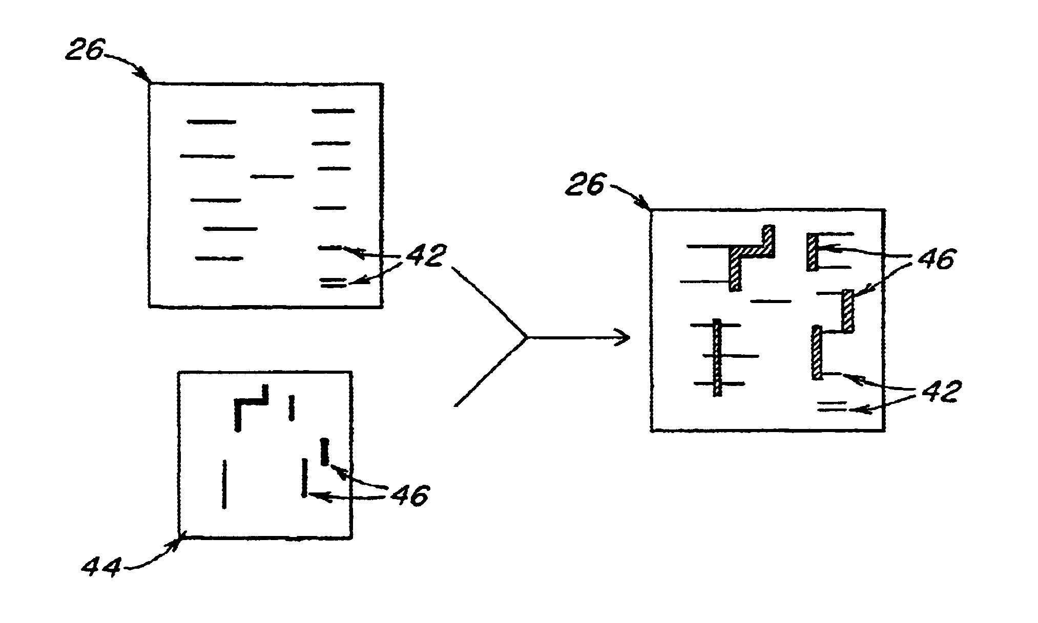
In the following description, the phrase, "lines," refers to either the trenches or the raised areas; e.g., plateaus; on a wafer. Moreover, the phrase, "contacts," refers to either the holes or pillars on a wafer. The described photoresists may either be a negative tone or a positive tone. The descriptions are applicable to either positive or negative imaging of the wafer or substrate.

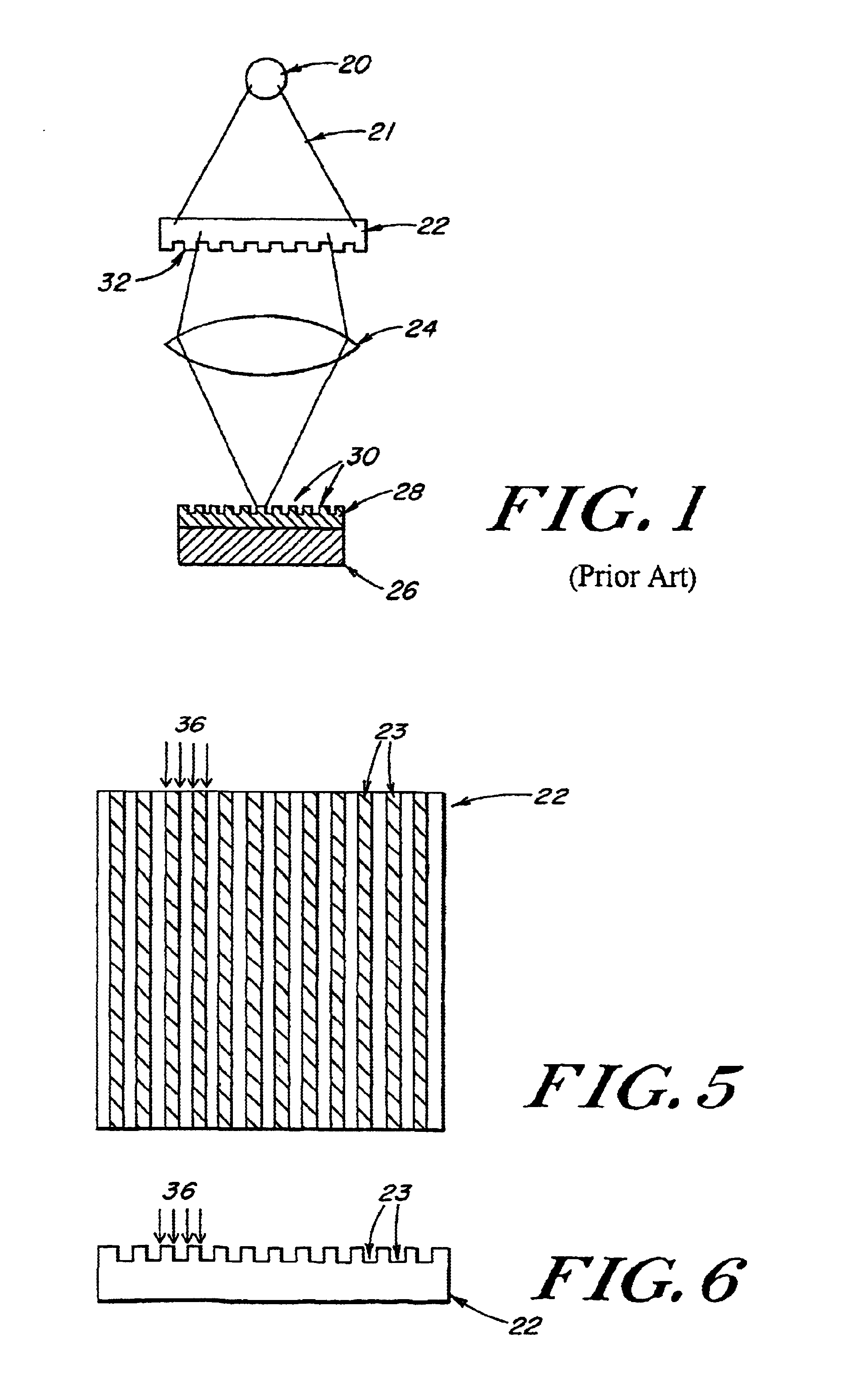
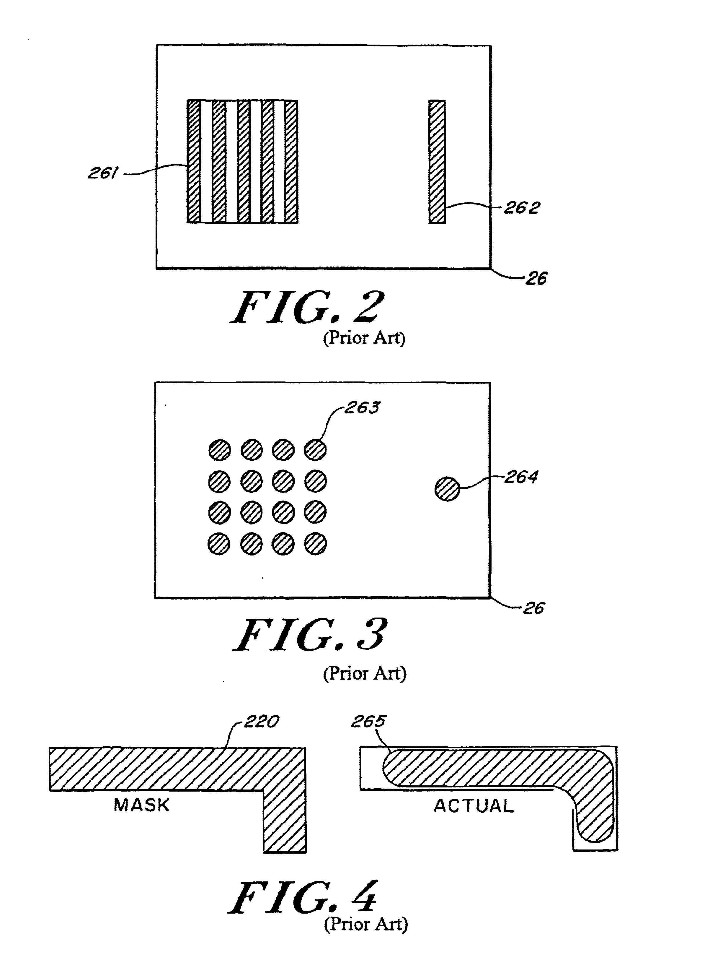
With respect to spatial frequency effects and optical proximity effects, any image that is lithographically exposed can be thought of in Fourier space, where components of various spatial frequencies sum to form the complete image. The lens acts as a low-pass filter because it ha...


PUM

PropertyMeasurementUnit
wavelengthaaaaaaaaaa
critical dimensionaaaaaaaaaa
densityaaaaaaaaaa

Abstract

A circuit fabrication and lithography process utilizes a mask including dense repetitive structures of features that result in a wide array of fine densely populated features on the exposed substrate film. Following this, a trimming procedure is performed to remove any unwanted fine patterned features providing multiple trimmed patterns on the substrate. An optional final step adds additional features as well as the interconnect features thus forming a circuit pattern. In this manner, all fine features may be generated using the exact same density of intensity patterns, and therefore, maximum consistency between features is established without the need for optical proximity correction. The secondary exposures are substantially independent from the initial dense-feature exposure in that the exposure of one set of features and the subsequent exposure of another set of features result in separate independent resist or masking layer reactions, thus minimizing corner rounding, line end shortening and other related spatial frequency effects and unwanted exposure memory effects.

Description

FIELD OF THE PRESENT INVENTIONThe present invention is directed to the fabrication of integrated circuits using arrays, gratings, and / or laser interferometry. More particularly, the present invention is directed to a process and methodology of fabricating integrated circuits that accounts for both optical proximity and spatial frequency effects while maintaining the resolution-enhancement characteristics required by sub-wavelength lithography.BACKGROUND OF THE PRESENT INVENTIONConventional optical projection lithography has been the standard silicon patterning technology for the past 20 years. It is an economical process due to its inherently high throughput thereby providing a desirable low cost per part or die produced. A considerable infrastructure (including steppers, photomasks, resists, metrology, etc) has been built up around this technology.In this process, a mask, or "reticle", includes a semiconductor circuit layout pattern typically formed of opaque chrome, on a transpare...

Claims


Application Information

Patent Timeline
Patent Type & Authority Patents(United States)
IPC IPC(8): G06F17/50G03F7/20G03F1/14G03F1/00
CPCG03F1/144G03F7/2026G03F7/70466G03F7/70441G03F7/70433G03F1/70
Inventor FRITZE, MICHAELTYRRELL, BRIAN
Owner MASSACHUSETTS INST OF TECH
Why Eureka
Try Eureka