Device and method for collecting and measuring chemical samples on pad surface in CMP

a technology of chemical samples and pads, applied in the field of semiconductor processing, can solve the problems of uneven planarization of wafers, affecting the so as to achieve more accurate and controlled sampling, the effect of improving the uniformity and uniformity of slurry distribution

Inactive Publication Date: 2005-01-04
MICRON TECH INC
View PDF24 Cites 5 Cited by
  • Summary
  • Abstract
  • Description
  • Claims
  • Application Information

AI Technical Summary

Benefits of technology

The present invention satisfies the aforementioned needs. The disclosed method and apparatus permit easier, more accurate, and more controlled sampling of the contaminants on a CMP pad.

Problems solved by technology

After a time, newly removed copper compounds, such as Cu(OH)2 and Cu(OH), clog and contaminate the CMP pad, thereby degrading its planarization effectiveness.
More specifically, as the CMP pad is used, contaminants build up within the pores or grooves of the CMP pad, thereby inhibiting an even distribution of slurry.
This could cause uneven planarization of the wafer and necessary wafer materials might be removed.
This method has several problems.
For example, pouring the solution on the pad in an uncontrolled manner may actually wash away contaminants from the area that will ultimately serve as the collection point.
As a result, the sample taken may not be a representative sample of the level of contaminants actually on the rest of the pad.
However, the pipette tips are generally too large to fit down into the narrow grooves on the CMP pad.
As a result, the sample taken may be inaccurate, and the user will likely make an inappropriate assessment of the CMP pad cleanliness.
Another problem is that the solvent may absorb into the CMP pad after it is poured.
As a result, it may be difficult to collect the required amount of solvent for testing.

Method used


Image

  • Device and method for collecting and measuring chemical samples on pad surface in CMP
  • Device and method for collecting and measuring chemical samples on pad surface in CMP
  • Device and method for collecting and measuring chemical samples on pad surface in CMP

Examples


Embodiment Construction

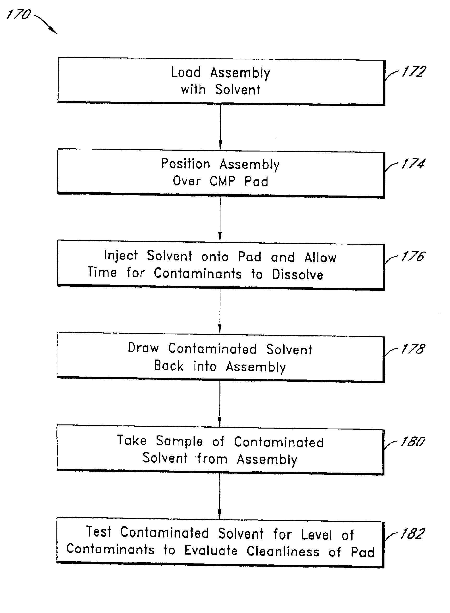
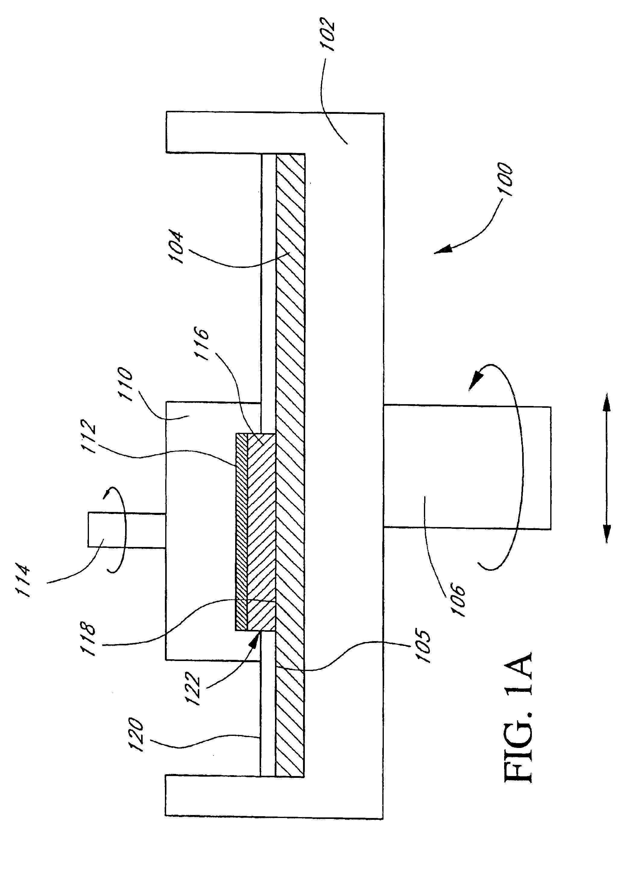
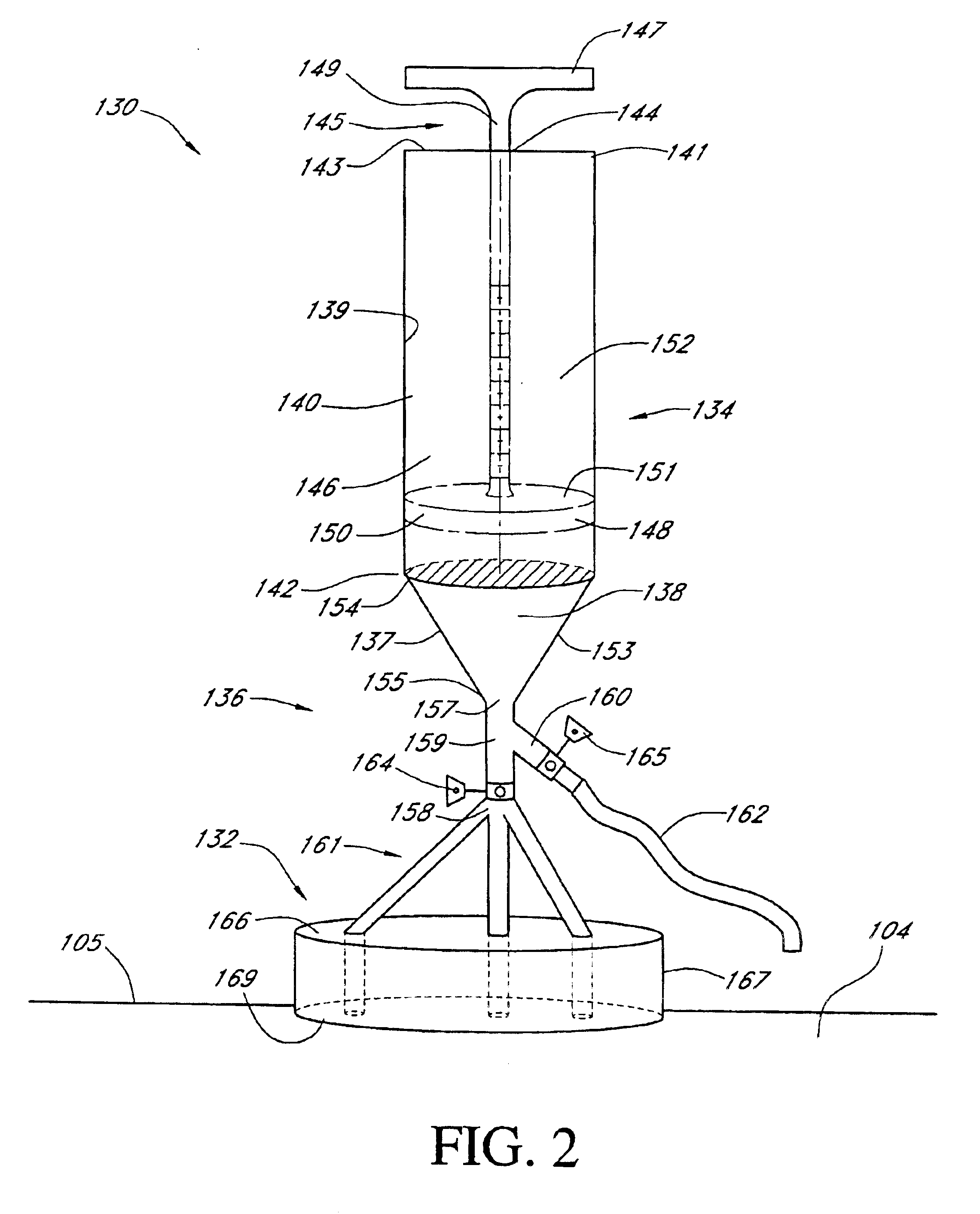
Reference will now be made to the drawings wherein like numerals refer to like parts throughout. Referring initially to FIG. 1, an exemplary CMP system 100 is illustrated. In particular, the CMP system 100 includes a platen 102 that is rotated about a shaft 106 by a motor (not shown). The platen 102 retains a polishing pad 104, and the CMP system 100 also includes a carriage 110 that has a wafer receiving surface 112 which is adapted to retain a wafer 116 within the carriage 110. The carriage 110 is also adapted to be rotated about a shaft 114 by a motor (not shown).

The operation of the CMP system 100 is similar to the operation of similar CMP systems of the prior art. Basically, the platen 102 is rotated and the carriage 110 is rotated such that rotational movement between the silicon wafer 116 and the polishing pad 104 is imposed. The platen 102 and the carriage 110 are then moved together such that an exposed surface 118 of the wafer 116 is brought into contact with an outer surf...


PUM

PropertyMeasurementUnit
diameteraaaaaaaaaa
ion coupled plasma analysisaaaaaaaaaa
solutionaaaaaaaaaa

Abstract

A chemical collection assembly and a method for using the assembly such that a chemical-mechanical polishing (CMP) pad used in the manufacture of semiconductor wafers can be assessed for cleanliness. The method involves delivering solvent from the assembly's reservoir to an enclosed volume over the CMP pad. The solvent then brings contaminants imbedded on the CMP pad into solution. This solution is then drawn back up from the enclosed volume wherefrom a sample of the solution can be taken. That sample is then analyzed for the level of contaminants present therein, and the analysis is compared to a pre-determined level of cleanliness to determine whether the CMP pad should or should not continue to be used for semiconductor wafer manufacturing.

Description

BACKGROUND OF THE INVENTION1. Field of the InventionThe present invention relates to semiconductor processing and, in particular, concerns a method of conditioning and measuring pads used in planarizing surfaces of a wafer using chemical-mechanical polishing.2. Description of the Related ArtChemical-mechanical polishing (CMP) is a technique whereby surfaces are planarized by the simultaneous application of both an etching and a polishing process. Semiconductor wafers are often globally planarized using CMP processing. In a typical CMP process, the semiconductor wafer is placed on a carriage, and a pad is positioned over the wafer to contact the upper surface of the semiconductor wafer. The carriage and the pad are further rotated in opposite directions, and a slurry containing an etchant and abrasive particles flows between the upper surface of the semiconductor wafer and the pad. The combination of the mechanical polishing of the pad and the chemical etching action involved in this...

Claims


Application Information

Patent Timeline
Patent Type & Authority Patents(United States)
IPC IPC(8): G01N1/32G01N1/02G01N33/00
CPCG01N1/32Y10T436/25625G01N2033/0095G01N2001/028
Inventor JOSLYN, MICHAEL J.
Owner MICRON TECH INC
Why Eureka
Try Eureka