Substrate with stacked vias and fine circuits thereon, and method for fabricating the same

a technology of fine circuits and vias, applied in the direction of printed circuit manufacturing, printed circuit aspects, printed element electric connection formation, etc., can solve the problems of limiting the design of printed circuit boards, affecting the production process, and affecting the quality of the produ

Inactive Publication Date: 2005-01-04
PHOENIX PRECISION TECH CORP +1
View PDF8 Cites 22 Cited by
  • Summary
  • Abstract
  • Description
  • Claims
  • Application Information

AI Technical Summary

Benefits of technology

Another objective of the present invention is to provide a substrate with stacked vias and fine circuits thereon for preventing the difficulties caused by surface roughening of the insulating layer surface during a conventional manufacturing process for making a substrate, so as to form a high density circuit layer.
Further another objective of the present invention is to provide a substrate with stacked via and fine circuits thereon for preventing the occurrence of resin residues formed in the opening of the holes during hole drilling and thereby solving the problem of poor electrical connection between the hole and the inner conductor or even wire breaking problem.
The substrate with stacked vias and fine circuits thereon disclosed in the present invention has only one surface of the core substrate being treated with build-up process, resulting an unsymmetrical structure. A surface roughening process is not required between the insulating layer and conductive circuit layer. Moreover, there is provided a photoimageable polymer, such as epoxy or polyimide as photoimageable insulating layer which is formed with a plurality of openings by using photolithography process, so as to prevent the occurrence of large amount of resin residues which causes poor electrical connection between the conductive vias and traces after electroplating or even generates traces breaking problem. The high density conductive circuit layer with fine circuits is then formed as a whole by assembling the conductive circuit layer on the lower surface of the core substrate and the through holes formed within the core substrate, together with the conductive vias and traces formed in the opening of a photoimageable insulating layer on the upper surface of the cores substrate.

Problems solved by technology

However, when the diameter of a hole is below 0.05 mm, the manufacturing process will become substantially difficult for implementation.
This thereby limits the design of printed circuit boards, to be even more highly dense.
However, if it is desired to further improve the traces dimension to even smaller scales, there will be manufacturing precision problems that cannot be overcome.
However this surface roughening process cannot be easily controlled and is particularly true for the substrate with fine circuits because as the effective bonding surface between the fine circuits and the insulating layer is largely reduced, the level of surface roughening must be increased to accommodate the reduced bonding capability which makes the overall manufacturing process more difficult.
In addition, when drilling a hole, it is very likely to create a large amount of resin residues, which is a major cause of poor electrical connection between the conductive vias and traces after electroplating.
This subsequently causes a disastrous effect or even leads to traces breaking, and as a result making the manufacturing process for the substrate more difficult and lowering the overall yield.

Method used


Image

  • Substrate with stacked vias and fine circuits thereon, and method for fabricating the same
  • Substrate with stacked vias and fine circuits thereon, and method for fabricating the same
  • Substrate with stacked vias and fine circuits thereon, and method for fabricating the same

Examples


Embodiment Construction

The foregoing objectives and advantages of the invention can be more fully understood by reference to the following detailed descriptions when taken in conjunction with the accompanying drawings. It is certain that the invention can be exemplified by using various other typed embodiments. The following preferred embodiments are only used for illustrating the invention and therefore should not limit the scope of the invention.

FIG. 5A to FIG. 5J illustrates the manufacturing method for making a multilayer printed circuit board in accordance with a preferred embodiment of the invention, which comprises a multilayer printed circuit board with the application of build-up process on surface of the core substrate for making an unsymmetrical multilayer printed circuit board.

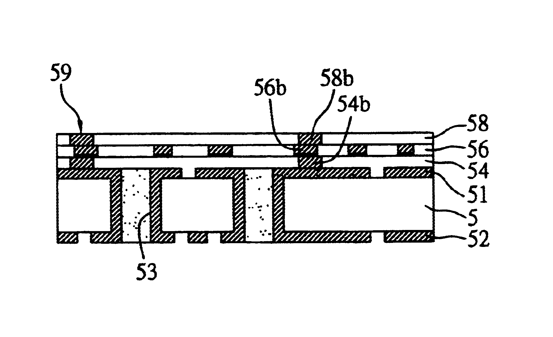
As shown in FIG. 5A, a core substrate 5 having an upper surface 5a and an opposing lower surface 5b is firstly provided in which a patterned first conductive circuit layer 51 and a metal layer 52 is formed on the top 5a ...


PUM

PropertyMeasurementUnit
diameteraaaaaaaaaa
diametersaaaaaaaaaa
conductiveaaaaaaaaaa

Abstract

A substrate with stacked vias and fine circuits and a method for fabricating the substrate are proposed. A core layer is formed with a metal layer respectively on upper and lower surfaces thereof, and at least one through hole. A first insulating layer is applied over the metal layer on the upper surface of the core layer and selectively formed with at least one first opening for exposing the metal layer. A metal layer is formed within the first opening, and a second insulating layer is applied over the first insulating layer and formed with a plurality of second openings, wherein the metal layer within the first opening is exposed via at least one second opening. After a conductive layer is applied over the second insulating layer and within the second openings, a metal layer is formed within the second openings. Finally, the conductive layer is removed by micro-etching.

Description

FIELD OF THE INVENTIONThe present invention relates to substrates of semiconductor packages, and more particularly, to an unsymmetrical multilayer circuit board having a build up layer on a single surface of a core layer thereof, and a method of making the same.BACKGROUND OF THE INVENTIONAs portable electronic devices are growing and are used in a wide variety of field such as in communication, internet and computer, semiconductor packages with high integrated circuits, smaller size and multi-leads such as those of BGA structure, flip chip structure, chip size package (CSP) and multichip module (MCM) are becoming more favorable. They are often incorporated with chips of high functionality such as microprocessors, multichip module, or drafting chips so as to perform instructions in higher speed. However, the manufacturing process for forming IC substrates of high I / O is often constrained as to assure preferable signal transmissions, improved bandwidth and resistance control and also ...

Claims


Application Information

Patent Timeline
Patent Type & Authority Patents(United States)
IPC IPC(8): H01L23/48H01L21/02H01L23/498H01L21/48H05K3/00H05K3/42H05K3/46
CPCH01L21/486H01L23/49822H01L23/49827H05K3/465H05K3/0023H05K3/423H05K3/4602H01L2924/0002H05K2201/09563H05K2201/0959H05K2201/096H01L2924/00
Inventor CHANG, RUEI-CHIH
Owner PHOENIX PRECISION TECH CORP
Why Eureka
Try Eureka