Compound semiconductor protection device for low voltage and high speed data lines

Inactive Publication Date: 2005-01-04
BANK OF AMERICA N A
View PDF18 Cites 6 Cited by
  • Summary
  • Abstract
  • Description
  • Claims
  • Application Information

AI Technical Summary

Benefits of technology

One embodiment of the protection circuit further includes a breakdown diode or transient voltage suppression (TVS) diode formed from a base-emitter junction of a transistor configured as the breakdown diode. Advantageously, the TVS diode can provide protection from undesired transients on a corresponding power supply line, such as VCC. The TVS diode A cathode of the breakdown diode is electrically coupled to the cathode of the first steering diode collection, and an anode of the breakdown diode is electrically cou

Problems solved by technology

Semiconductor devices can be permanently damaged when exposed to an undesired voltage transient such as electrostatic discharge (ESD).
However, conventional techniques developed for silicon

Method used


Image

  • Compound semiconductor protection device for low voltage and high speed data lines
  • Compound semiconductor protection device for low voltage and high speed data lines
  • Compound semiconductor protection device for low voltage and high speed data lines

Examples


Example

Although this invention will be described in terms of certain preferred embodiments, other embodiments that are apparent to those of ordinary skill in the art, including embodiments which do not provide all of the benefits and features set forth herein, are also within the scope of this invention. Accordingly, the scope of the invention is defined only by reference to the appended claims.

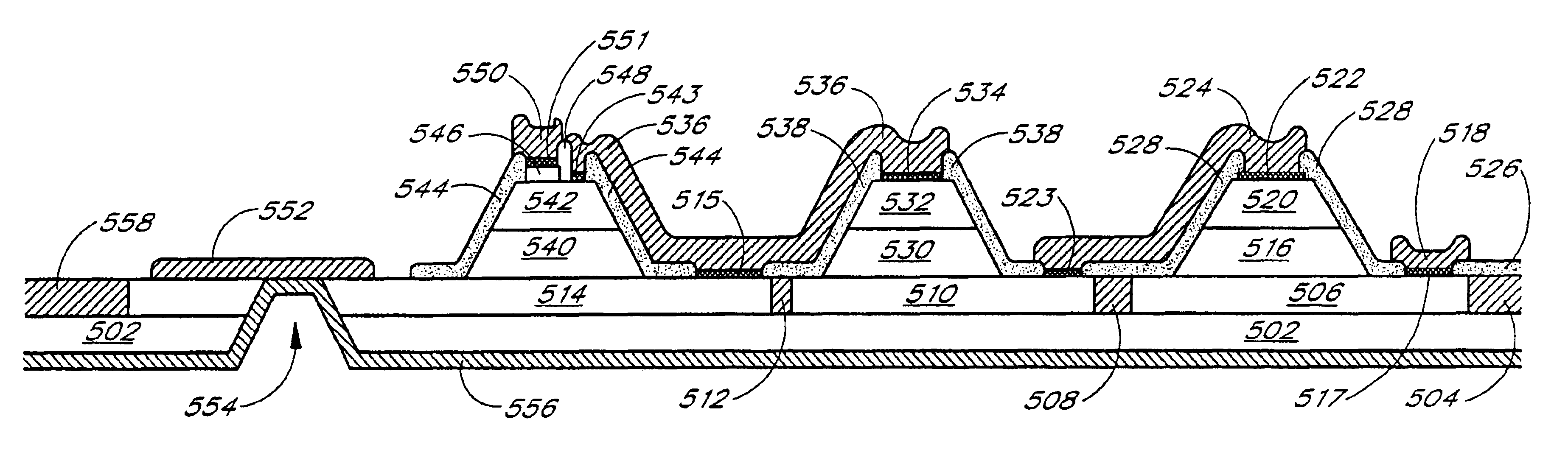
While illustrated in the context of gallium arsenide (GaAs), the skilled artisan will appreciate that the principles and advantages described herein are applicable to other types of epitaxial wafers, including epitaxial wafers fabricated from indium phosphide (InP) and the like.

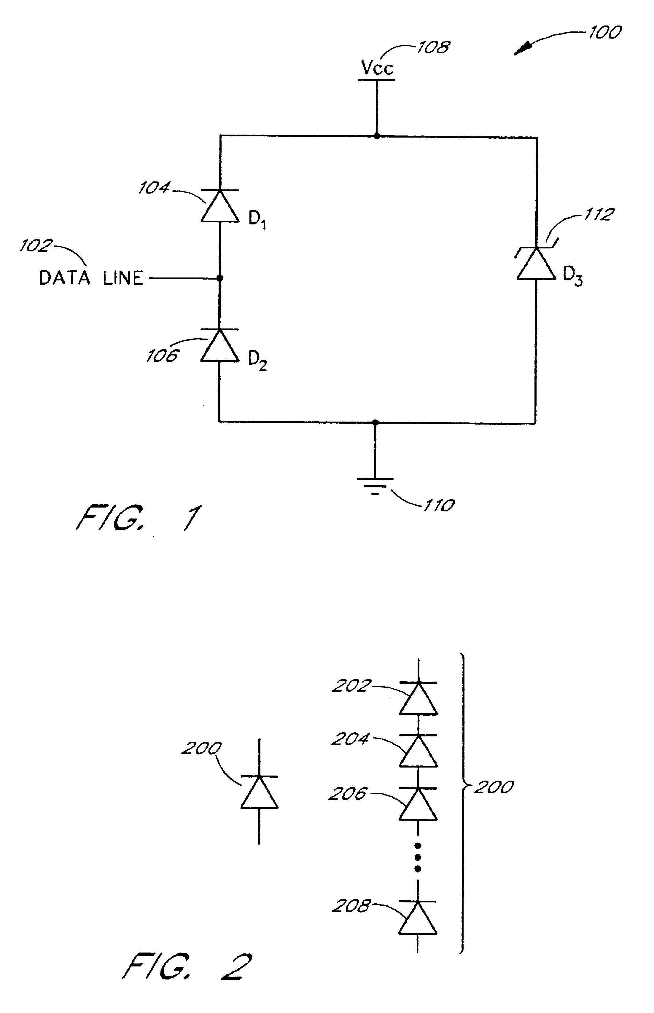
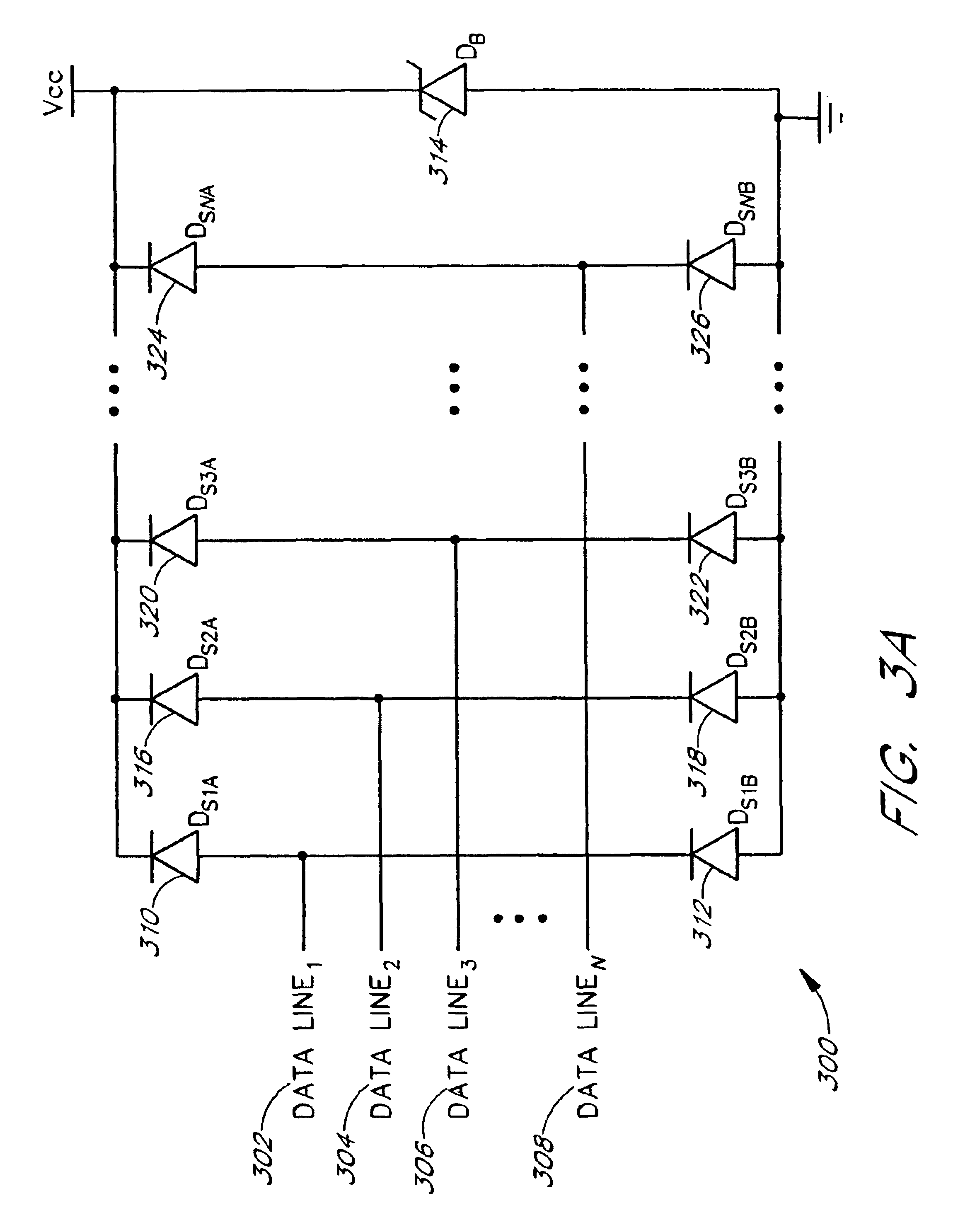
FIG. 1 illustrates a transient voltage protection circuit 100 according to an embodiment the invention. The transient voltage protection circuit 100 limits an undesired voltage transient on a data line 102 to a safe level to protect transistors and other devices that are electrically coupled to the data line 102.

The data line...


PUM


Abstract

The invention relates to the protection of devices in a monolithic chip fabricated from an epitaxial wafer, such as a wafer for a Group III-V compound semiconductor or a wafer for a Group IV compound semiconductor. Devices fabricated from Group III-V compound semiconductors offer higher speed and better isolation than comparable devices from silicon semiconductors. Semiconductor devices can be permanently damaged when exposed to an undesired voltage transient such as electrostatic discharge (ESD). However, conventional techniques developed for silicon devices are not compatible with processing techniques for Group III-V compound semiconductors, such as gallium arsenide (GaAs). Embodiments of the invention advantageously include transient voltage protection circuits that are relatively efficiently and reliably manufactured to protect sensitive devices from undesired voltage transients. A protection circuit can be monolithically integrated with the protected circuit or can be packaged in a separate integrated circuit.

Description

BACKGROUND OF THE INVENTION1. Field of the InventionThe invention generally relates to compound semiconductors. In particular, the invention relates to the protection of circuits from undesired transient voltage spikes such as those from electrostatic discharge (ESD).2. Description of the Related ArtAn undesired voltage transient on a data line can damage an electronic circuit. As technology progresses and device geometries continue to shrink, devices become ever more sensitive to voltage transients. One example of a source of an undesired voltage transient is electrostatic discharge (ESD).Steering diodes and transient voltage suppressors have been applied to data lines in conventional circuits implemented in silicon. Where such steering diodes and / or transient voltage suppressors are fabricated from silicon on a monolithic chip, pnpn or npnp thyristor latchup can occur, which can also damage the electronic circuit. Although incorporating discrete diodes and transient voltage suppre...

Claims


Application Information

Patent Timeline
IPC IPC(8): H01L21/70H01L21/8252H01L27/06
CPCH01L27/0605H01L21/8252
Inventor BARKHORDARIAN, VREJ
Owner BANK OF AMERICA N A
Why Eureka
Try Eureka