Leadframe for integrated circuit chips having low resistance connections

a technology of integrated circuit chips and leadframes, which is applied in the direction of electrical equipment, electrical apparatus, electrical apparatus, etc., can solve the problems of leadframes whose spacing and dimensions are limited, increase in length, and inability to appear to be possible, so as to reduce the length of the larger-diameter wires for connection between the semiconductor chip and the leadframe, the effect of reducing the electrical resistan

Inactive Publication Date: 2005-01-04
STMICROELECTRONICS SRL
View PDF14 Cites 5 Cited by
  • Summary
  • Abstract
  • Description
  • Claims
  • Application Information

AI Technical Summary

Benefits of technology

Embodiments of the present invention further provide a leadframe for semiconductor chips which has a minimized electrical resistance and is particularly suitable for use with chips which require...

Problems solved by technology

Chip leadframes, however, have leads whose spacing and dimensions are limited by the mechanical stamping capabilities of the devices meant to manufacture the leadframes.
Moreover, in the case of an application with leadframes which require wires having two diameters, a larger one for the power section and a smaller one for the signal section, for the wires that must withstand high power levels (i.e., the larger-diameter ones) it is preferable to reduce the resistance as much as possible, but this does not appear to be possible with currently known leadframes.
Moreover, in the case of a...

Method used


Image

  • Leadframe for integrated circuit chips having low resistance connections
  • Leadframe for integrated circuit chips having low resistance connections

Examples


Embodiment Construction

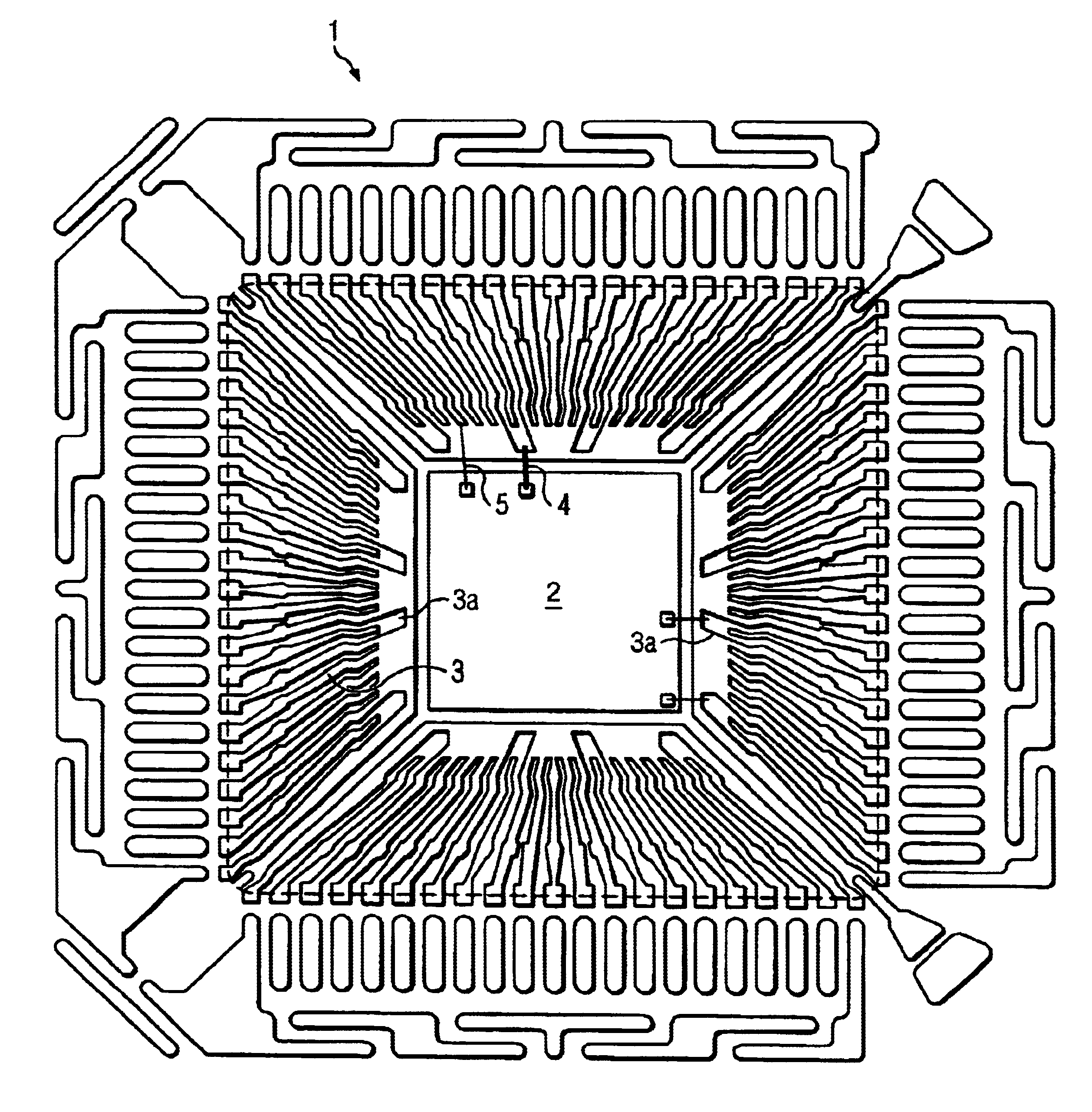
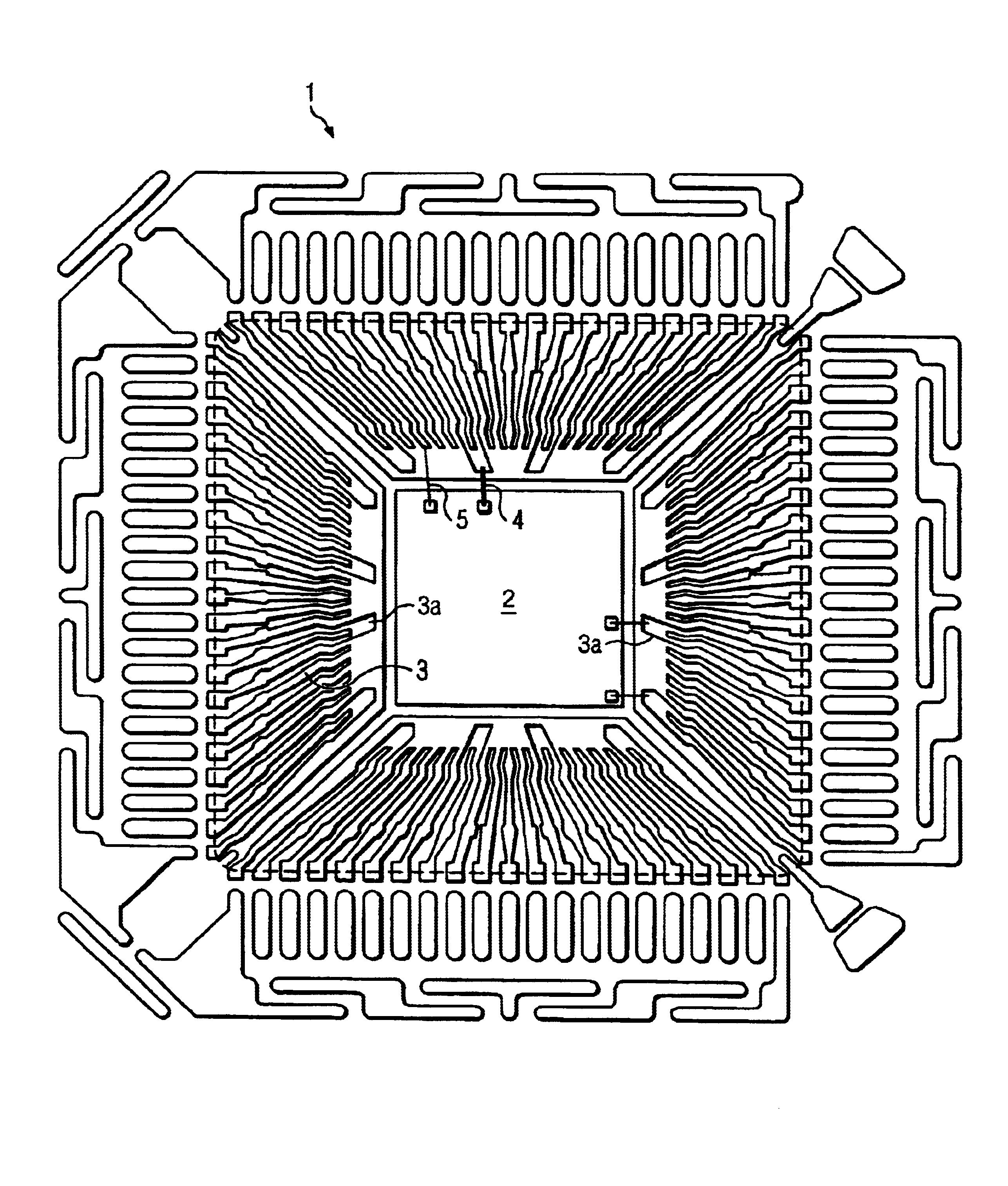
With reference to the only FIGURE cited above, the leadframe for semiconductor chip, generally designated by the reference numeral 1, is constituted by a stamped frame made of metallic material which supports, at a central region, a semiconductor chip 2 which is to be connected to the leadframe by means of connecting wires, such as bond wires, which can have different diameters according to the type of connection, power level or input / output signal.

The leadframe 1 is provided with a plurality of leads 3 which are arranged so as to substantially surround the semiconductor chip, and a connection between the semiconductor chip 2 and the leadframe 1 corresponds to each lead. As can be seen in the drawing, leads 3 are disposed along each side of semiconductor chip 2.

Leadframe 1 is provided with leads 3 having at least two different lengths. In the FIGURE, the reference numeral 3a designates a lead that is longer than the leads designated by the reference numeral 3.

In this case, as clearl...


PUM


Abstract

A leadframe for semiconductor devices, including a region which is adapted to support a semiconductor device and a plurality of leads which are arranged so as to be directed toward the region, for mutual connection, by connecting wires connecting the leads and the semiconductor device. The leads include leads having at least two different lengths for the connection of connecting wires having different diameters.

Description

BACKGROUND OF THE INVENTION1. Technical Field of the InventionThe present invention relates to a leadframe for chips, having low-resistance connections.2. Description of the Related ArtIt is known that the manufacture of integrated-circuit devices provides for a metallic supporting frame (leadframe) on which the semiconductor chip is placed and appropriately connected to the leadframe by means of wires.The current trend is to increasingly miniaturize chips, which accordingly have high efficiency as regards their electrical resistance.Chip leadframes, however, have leads whose spacing and dimensions are limited by the mechanical stamping capabilities of the devices meant to manufacture the leadframes.Consequently, the ever-smaller chips are connected on chip supporting pads having correspondingly reduced dimensions, but the leads of the leadframes are distant from the chip.Consequently, the electrical resistance of the chip is determined not only by the electrical resistance of the s...

Claims


Application Information

Patent Timeline
IPC IPC(8): H01L23/495H01L23/48
CPCH01L23/49541H01L2224/48091H01L2224/48247H01L2224/45144H01L2924/10253H01L2924/00014H01L2924/00
Inventor TIZIANI, ROBERTOCOGNETTI, CARLOCIGADA, ANDREA
Owner STMICROELECTRONICS SRL
Why Eureka
Try Eureka