
Method for controlling column decoder enable timing in synchronous semiconductor device and apparatus thereof

a technology of synchronous semiconductor devices and decoders, applied in the direction of information storage, static storage, digital storage, etc., can solve the problem that users cannot increase the maximum operating frequency of an sdram having a cl of 2 and achieve the effect of increasing the maximum operating frequency

Inactive Publication Date: 2005-01-04
SAMSUNG ELECTRONICS CO LTD
View PDF6 Cites 17 Cited by
  • Summary
  • Abstract
  • Description
  • Claims
  • Application Information

AI Technical Summary

Benefits of technology

This approach enhances the maximum operating frequency of semiconductor memory devices by optimizing delay times based on the presence of gaps between command signals, improving performance during write-read operations without compromising data integrity.

Problems solved by technology

Therefore, a user cannot increase the maximum operating frequency of an SDRAM having a CL of 2 in the case of performing write-read operations in order.

Method used


Image

  • Method for controlling column decoder enable timing in synchronous semiconductor device and apparatus thereof
  • Method for controlling column decoder enable timing in synchronous semiconductor device and apparatus thereof
  • Method for controlling column decoder enable timing in synchronous semiconductor device and apparatus thereof

Examples


Embodiment Construction

The present invention will now be described more fully with reference to the accompanying drawings, in which exemplary embodiments of the invention are shown. This invention may, however, be embodied in many different forms and should not be construed as being limited to the exemplary embodiments set forth herein; rather, these exemplary embodiments are provided so that this disclosure will be thorough and complete and, will fully convey the concept of the present invention to those skilled in the art. In the drawings, the thickness of layers and regions are exaggerated for clarity. Like reference numerals in different drawings refer to like elements.

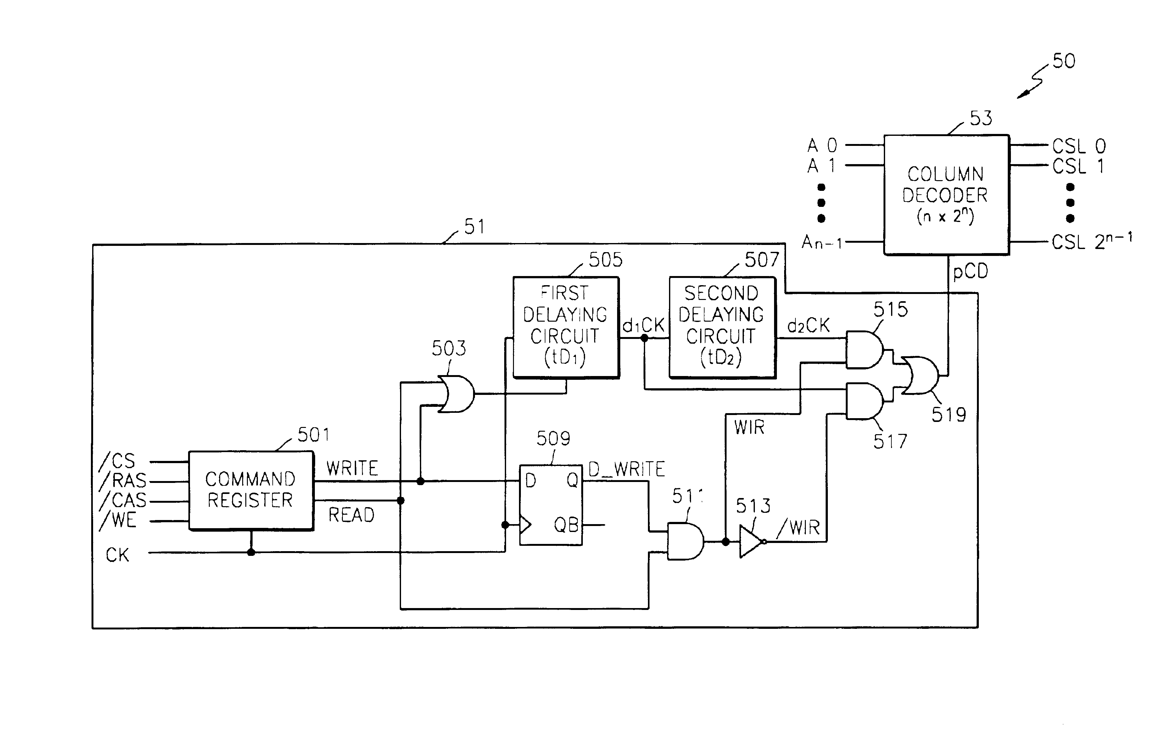
FIG. 5 is a block diagram of a column selection circuit 50 according to an exemplary embodiment of the present invention. Referring to FIG. 5, the column selection circuit 50 includes a timing control signal generating circuit 51 and a column decoder 53.

The timing control signal generating circuit 51 delays the clock signal CK for a des...


PUM


Abstract

A method for controlling column decoder enable timing including determining if there is a gap between a data write command and a data read command which occur consecutively; generating a timing control signal for delaying received clock signal for an amount of time which depends on the determination result; and activating a column decoder in response to the timing control signal. Generating a timing control signal includes generating a timing control signal having a first delay time if there is a gap and generating a timing control signal having a second delay time if there is no gap, when the first delay time is shorter than the second delay time. An effect is an increase in the maximum operating frequency of a system for outputting data.

Description

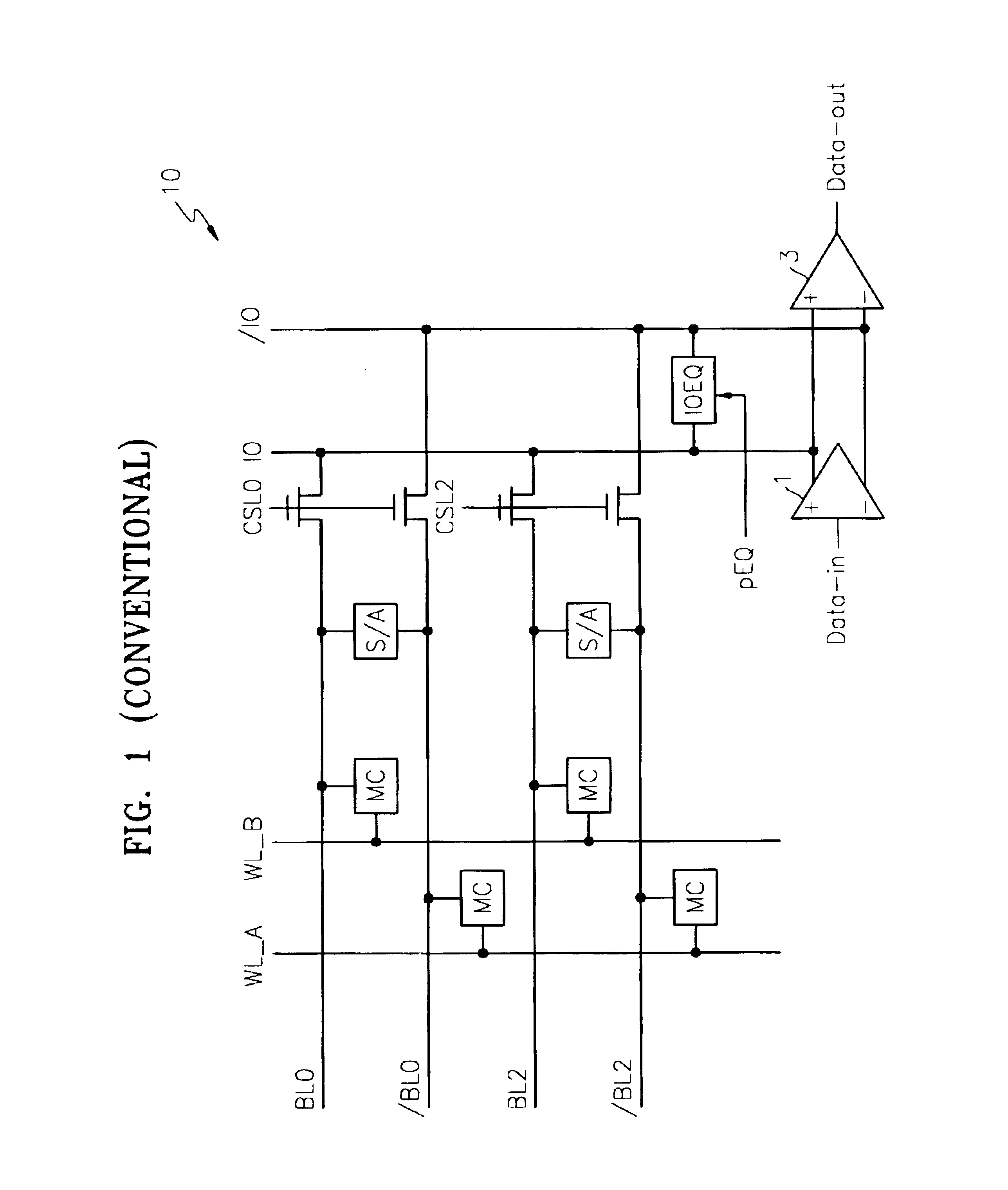
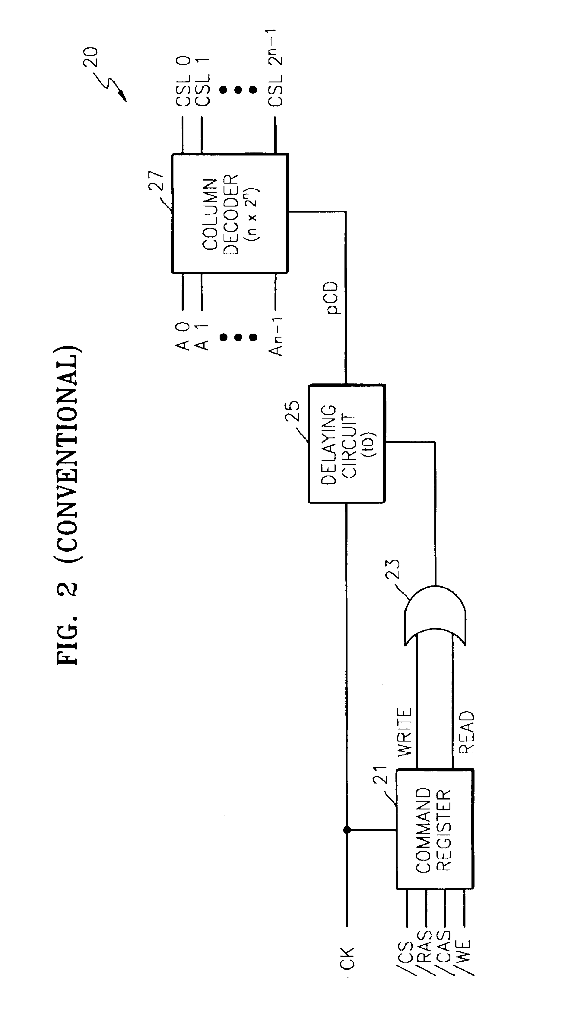
BACKGROUND OF THE INVENTION1. Field of the InventionThe present invention relates to a semiconductor memory device, and more particularly, to a method and a device for increasing a maximum operating frequency if there is a gap between a data write command signal and a data read command signal.2. Description of the Related ArtFIG. 1 is a schematic data input and output circuit 10 of a conventional DRAM. The input and output circuit 10 of FIG. 1 includes bit lines BLO, / BLO (“ / ” indicates an active low), BL2 and / BL2, memory cells MC contacting intersection points of word lines WL_A and WL_B, sensing amplifiers S / A, data input and output lines IO and / IO, equalizing circuits IO EQ for equalizing the data input and output lines IO and / IO, a data input buffer 1, and a data output buffer 3. The equalizing circuits IO EQ are activated in response to a control signal pEQ.FIG. 2 is a block diagram of a conventional column selection circuit. The column selection circuit 20 includes a comman...

Claims


Application Information

Patent Timeline
Patent Type & Authority Patents(United States)
IPC IPC(8): G11C11/408G11C7/00G11C7/22G11C11/407G11C11/4076
CPCG11C7/22G11C11/4087G11C11/4076
Inventor SHIN, CHOONG-SUN
Owner SAMSUNG ELECTRONICS CO LTD
Learn More