Method and system for processing a semi-conductor device

a semi-conductor device and processing method technology, applied in the field of semi-conductor device processing and system, can solve the problems of reducing the operation efficiency generating errors in the accuracy of projection exposure tools, and reducing so as to improve the overlay accuracy of device area, improve the yield and productivity of semi-conductor devices, and enhance the functioning of semiconductor devices

Inactive Publication Date: 2005-01-11
HITACHI LTD
View PDF2 Cites 74 Cited by
  • Summary
  • Abstract
  • Description
  • Claims
  • Application Information

AI Technical Summary

Benefits of technology

With the intention of overcoming the foregoing problem, it is an object of the present invention to provide a method and system for processing a semi-conductor device which are capable of improving the overlay accur

Problems solved by technology

The production line of semiconductor devices has the installation of multiple projection exposure tools in general, and there exists the disparity of accuracy among these projection exposure tools.
On this account, when the mix-and-match exposure, the so-called overlap exposure is carried out among multiple exposure tools, the disparity of accuracy among the exposure tools is generated error among layers called “matching error” in a product of the semiconductor device.
A scheme of preventing the matching error is using the same projection exposure tool throughout all steps of semiconductor device production process; however, it results in a lower o

Method used


Image

  • Method and system for processing a semi-conductor device
  • Method and system for processing a semi-conductor device
  • Method and system for processing a semi-conductor device

Examples


first embodiment

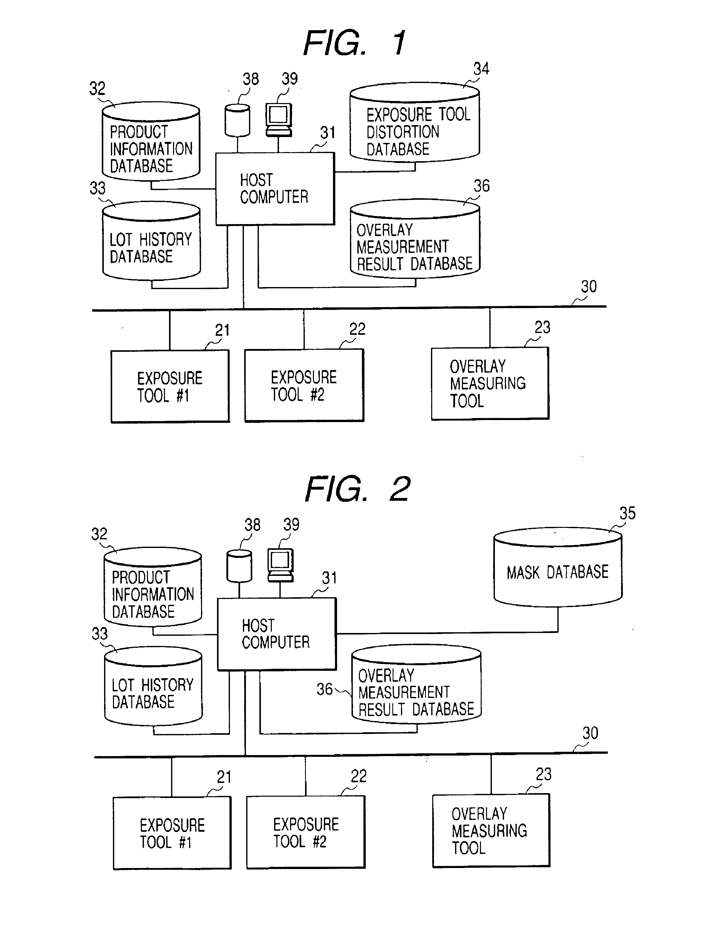
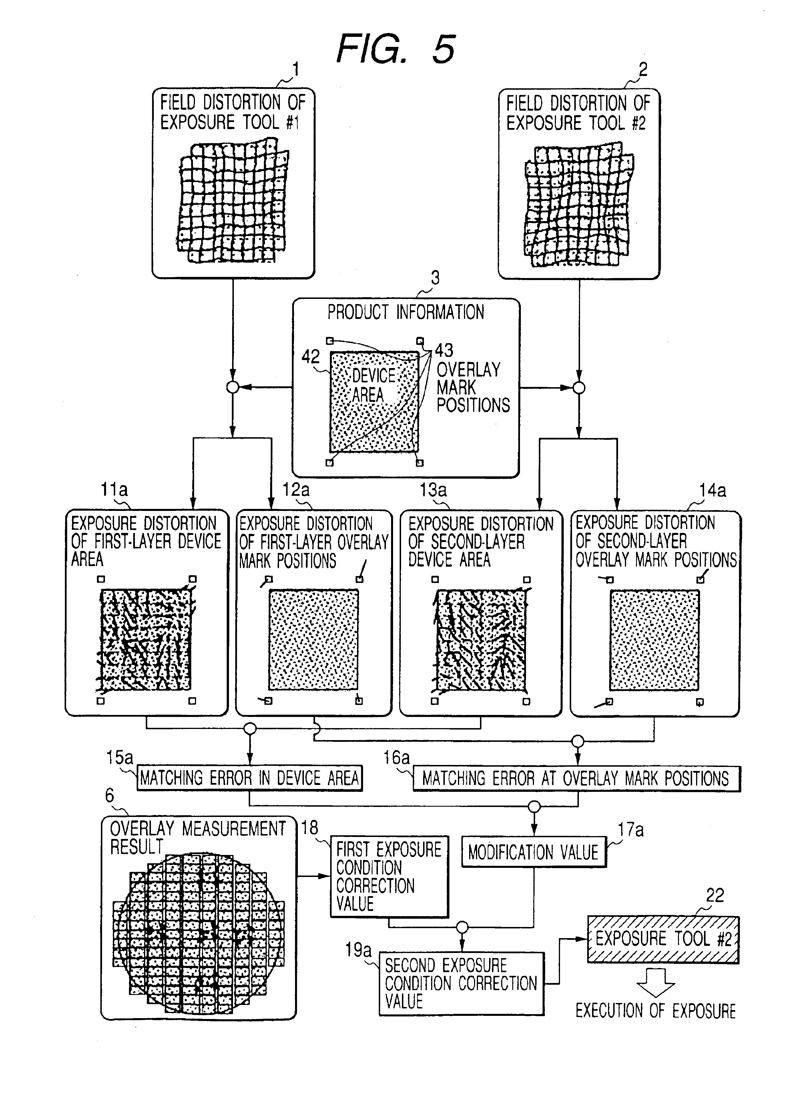
First of all, explanation will be given on the first embodiment of the apparatus (system) for conducting matching error compensation upon exposure field strain in the exposure tool according to the present invention, by referring to FIGS. 1 and 5. In the figures, a reference numeral 31 is a host computer, in which various kinds of processing are executed. A reference numeral 32 is a product information database, holding and storing therein, design data such as device areas of the semiconductor device products and overlay measuring mark positions, etc., into which design information of the products (the semiconductor products) is inputted as the design information from a CAD system (not shown in the figure), for example, through a network 30.

A reference numeral 33 is a lot history database, holding and storing therein history data of indicating which one of the projection exposure tools (apparatuses) and which one of the masks are used in each of the steps, and is inputted from a pro...

second embodiment

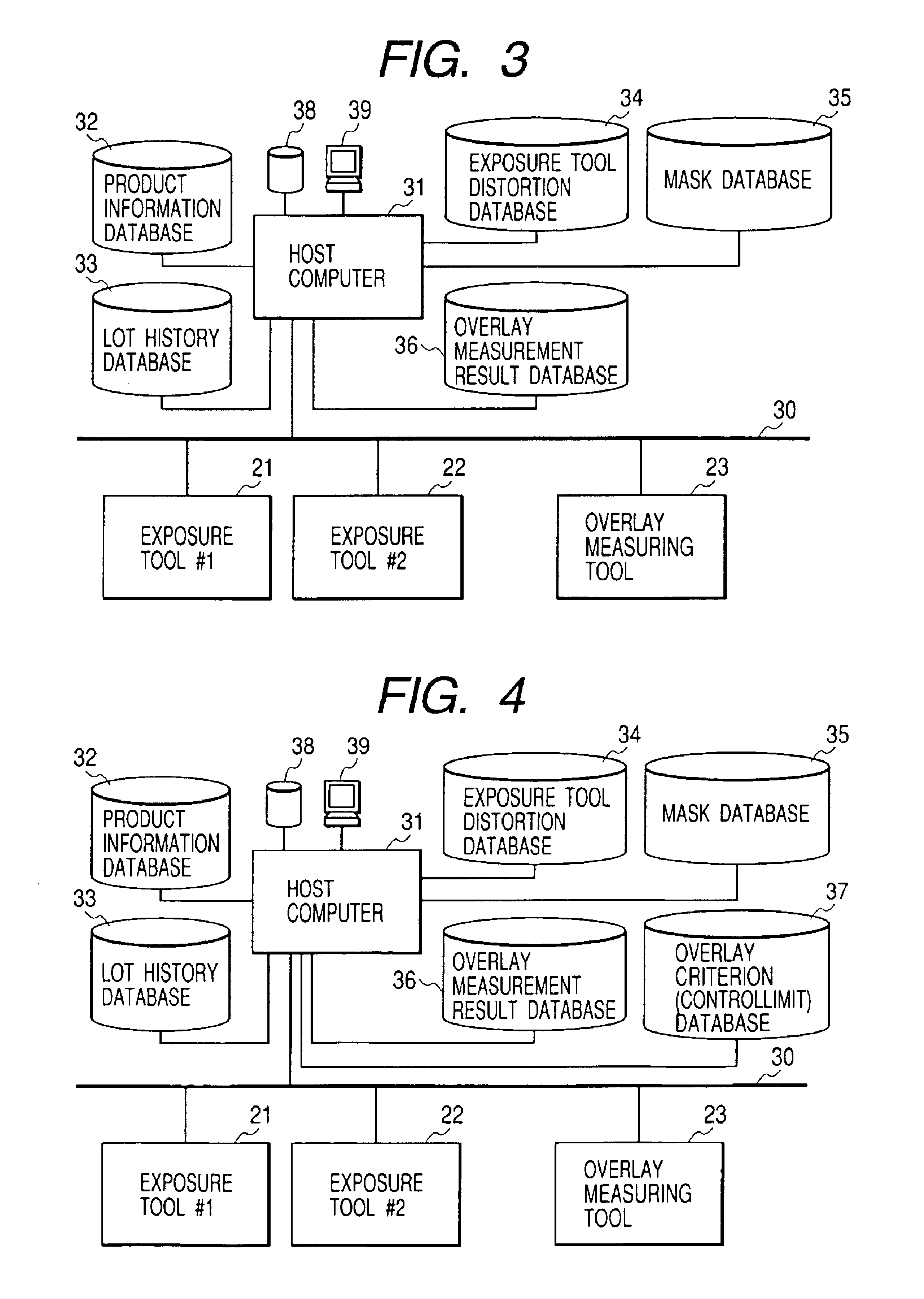
Next, the second embodiment of invention which pertains to a system for matching error correction for the masks fitted to the exposure tools will be explained with reference to FIG. 2 and FIG. 6.

This embodiment differs from the first embodiment in that a mask accuracy database 35 which stores patterns of device area on the masks and the measurement result of position error of overlay measurement marks is installed in place of the exposure tool distortion database 34. In carrying out the exposure of one layer (second layer) of a semiconductor device, the host computer 31 searches the mask accuracy database 35 to get data 5 and 4 of patterns of device area and position error of overlay measurement marks of the mask to be used for the immediate layer (second layer) and the mask which has been used for the former layer (first layer) based on the coordinate data of the device area 42 and position data of the overlay measurement marks 43 taken out as product information 3 from the product...

third embodiment

Next, the third embodiment of invention which pertains to a system for matching error correction against the exposure field distortion of exposure tools and the masks fitted to the exposure tools will be explained with reference to FIG. 3 and FIG. 7. This embodiment combines the first and second embodiments for dealing with the disparity among the masks as well as among the exposure tools encountered in the mix-and-match exposure.

FIG. 3 explains the system of implementing the matching error correction against the exposure field distortion of exposure tools and the masks. This embodiment differs from the first and second embodiments in that it includes both the exposure tool distortion database 34 shown in FIG. 1 and the mask accuracy database 35 shown in FIG. 2. In carrying out the exposure of one exposure layer (second layer) of a semiconductor device, as shown in FIG. 7, the host computer 31 searches the exposure tool distortion database 34 to get exposure field distortion data 2 ...


PUM


Abstract

A method and a system for processing a semiconductor device intended to improve the overlay accuracy of a semiconductor device product, particularly in its device area, in carrying out the mix-and-match exposure process are designed to calculate the difference of exposure distortions between two layers in the device area and the difference of exposure distortions between the two layers at the overlay measurement mark position from data of exposure field distortions of two exposure tools used for the mix-and-match exposure process and data of device area and overlay measurement mark position of the product, calculate a modification value which relates both differences to each other, calculate a first exposure condition correction value from the measurement result of overlay, and carry out the exposure process based on a second exposure condition correction value which is evaluated by modifying the first exposure condition correction value with the modification value.

Description

BACKGROUND OF THE INVENTIONThe present invention relates to a method and system for processing (producing) a semi-conductor device, and particularly to a technique for improving the accuracy of overlay at the mix-and-match exposure process in which different exposure tools are used for different layers on a semiconductor substrate.In the recent trends of higher integration and enhanced functioning of semiconductor devices, the production process is required to be much more accurate for accomplishing these demands. On the other hand, reduction of the production cost of semiconductor devices is another crucial subject.In the production process of a semiconductor device, circuit patterns formed on exposure masks (will be termed simply “masks”) are transferred on to a semiconductor wafer (will be termed simply “wafer”) which is coated with photo-resist by using a projection exposure tool (apparatus). As a semiconductor device is made circuit patterns on multiple layers, the circuit patt...

Claims


Application Information

Patent Timeline
IPC IPC(8): G03F7/20H01L21/027
CPCG03F7/70458G03F7/70525G03F7/70633G03F7/70591G03F7/70533
Inventor MATSUMOTO, SHUNICHIYOSHITAKE, YASUHIROMIYAMOTO, YOSHIYUKI
Owner HITACHI LTD
Why Eureka
Try Eureka