Method for fabricating a deep trench capacitor for dynamic memory cells

a technology of dynamic memory cells and capacitors, which is applied in the direction of semiconductor devices, electrical apparatus, transistors, etc., can solve the problems of increasing the depth of the trench, increasing the difficulty of etching, and increasing the technical difficulty, so as to reduce the process complexity

Inactive Publication Date: 2005-01-11
POLARIS INNOVATIONS
View PDF10 Cites 14 Cited by
  • Summary
  • Abstract
  • Description
  • Claims
  • Application Information

AI Technical Summary

Benefits of technology

One configuration of the method may considerably reduce the process complexity compared to the selective introduction. In this configuration, there is provision for the collar region, prior to the application of the grains, to be provided with a layer which masks the collar region and for the grains to be removed in the region close to the top side prior to the subsequent processes and for the masking layer to be removed again after the doping. This masking layer enables the coating with the grains initially to be carried out in a non-selective manner, since this coating can then be removed again.
However, the configuration of the method with a masked layer also makes it possible to use other subsequent process steps. For example, in a variant, there is provision for the doping to be produced by means of an As vapor diffusion step. This makes it possible to overcome the difficulty of achieving a minimum As glass layer thickness which arises in particular with feature sizes of less than 130 nm. However, in the case of As vapor diffusion, the collar region has to be reliably masked, which is ensured by the masked layer which is applied in this configuration of the method according to the invention.

Problems solved by technology

This presents difficulties for feature sizes of less than 130 nm, since the demands for a minimum thickness can no longer be satisfied on account of the high aspect ratio of the trench structure, which is greater than 50, and the fact that the deposition conformity of the As CVD process used to produce the As glass layer is far from ideal.
an increase in the depth of the trench, which has hitherto been the most important measure in capacitor scaling but presenting increasing technical difficulties with scaling of the trench cross section,
selecting a bottle-shaped cross section for the trench, known as a bottle shaped capacitor, but this presents increasing etching difficulties in view of the aim to achieve a short distance between the trenches,
a reduction in the thickness of the dielectric, but this is limited by incipient charge carrier tunneling,
an increase in the roughness of the (internal) trench surface by means of pore etching (mesopores), which it has not to date been possible to achieve on account of the tight tolerances imposed on the mesopores.

Method used


Image

  • Method for fabricating a deep trench capacitor for dynamic memory cells
  • Method for fabricating a deep trench capacitor for dynamic memory cells

Examples


Embodiment Construction

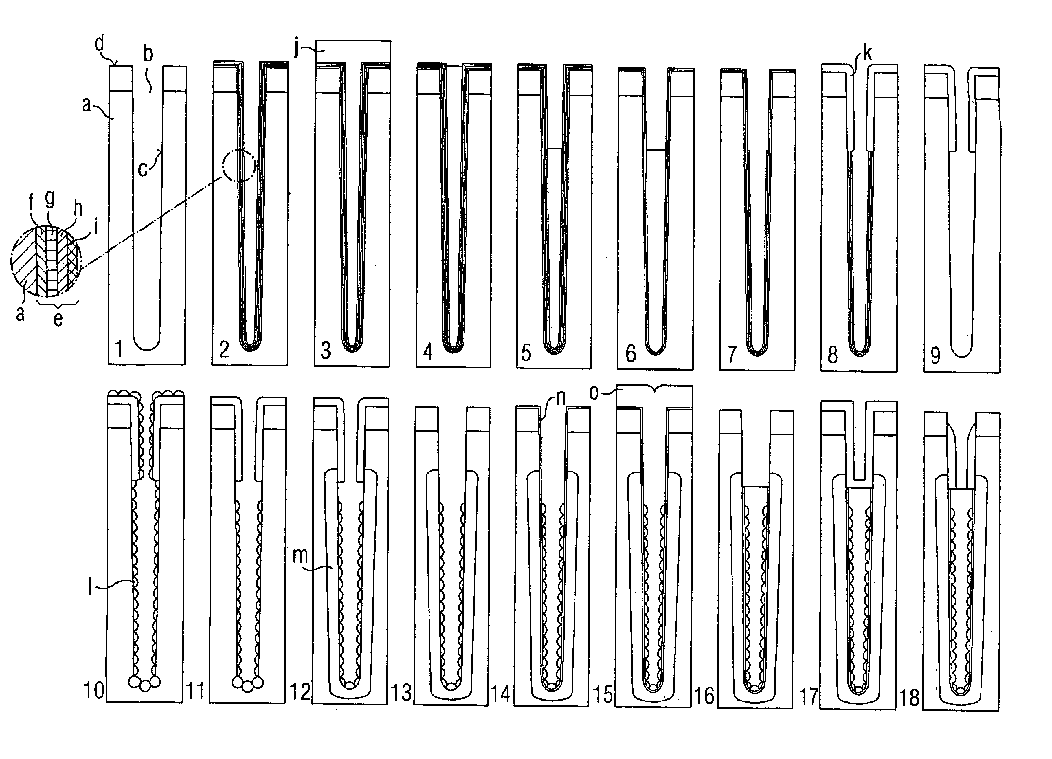
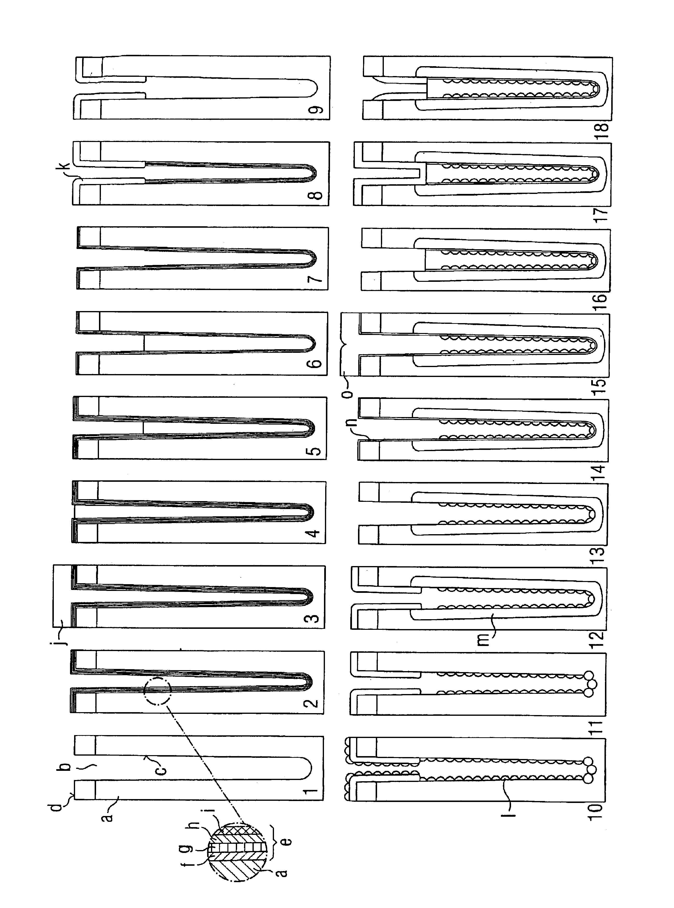
The exemplary embodiment relates to the configuration of the method according to the invention with the non-selective application of grains using a layer which masks the collar region.

In process step 1, a trench structure, i.e. the trench b, is produced in a conventional way in a silicon substrate a. In step 2 a thin mask layer e is deposited on the inner surface c of the trench b and on the substrate top surface d.

The thin mask layer is distinguished by the fact that it can be removed selectively with respect to the surface c of the trench b and is not oxidized or is only oxidized to an insignificant extent during a step of oxidizing the surface c which is required during the further integration process.

In an advantageous embodiment, this thin mask layer e comprises a layer sequence made up of a first layer f, preferably oxide, a second layer g, preferably Si nitride, a third layer h, preferably amorphous silicon, and a fourth layer i, preferably Si nitride.

This layer sequence is d...


PUM


Abstract

A method for fabricating a deep trench capacitor for dynamic memory cells in which a trench is etched into the depth of a semiconductor substrate, and wherein the interior of the trench is provided with a doping and a dielectric and is filled with a conductive material as an inner electrode. The inner electrode and the dielectric are etched back within a collar region, and a collar is formed using a collar process comprising a collar oxide deposition and etching back of the collar oxide on the substrate surface and in the trench as far as the inner electrode, after which the inner electrode is completed by further steps of depositing and etching back conductive layers. Prior to the doping a masking layer is applied to the collar region of the trench, and this masking layer is removed again before the collar process. Before the dielectric is applied the surface of the lower regions of the trench outside the collar region a layer of grains of conductive material is applied.

Description

BACKGROUND OF THE INVENTIONThe invention relates to a method for fabricating a deep trench capacitor for dynamic memory cells, in which a trench is etched into a semiconductor substrate. In the interior, i.e., below a collar region near the top surface of the substrate, there is provided a doping and a dielectric. Then, the trench which which includes the doping and dielectric is filled with a conductive material to form an inner electrode. The inner electrode and the dielectric are etched away within the collar region, and a collar is formed using a collar process, comprising a collar oxide deposition and etching back of the collar oxide on the substrate surface and in the trench as far as the inner electrode. Then, the inner electrode is completed by further steps of depositing and etching back conductive layers.Complex integrated circuits of dynamic memory chips have integrated capacitor structures formed using one of three different designs,planar metal-insulator-silicon, double...

Claims


Application Information

Patent Timeline
Patent Type & Authority Patents(United States)
IPC IPC(8): H01L21/02H01L21/20H01L21/70H01L21/8242
CPCH01L27/1087H10B12/0387
Inventor TEMMLER, DIETMARKRASEMANN, ANKE
Owner POLARIS INNOVATIONS
Why Eureka
Try Eureka