Maskless photon-electron spot-grid array printer

a photon-electron and array printer technology, applied in photomechanical equipment, instruments, nuclear engineering, etc., can solve the problems of limiting stochastic coulomb interactions between individual particles, increasing difficulty and cost of masks used in image-projection systems, and extremely difficult and expensive masks for electron-projection systems

Inactive Publication Date: 2005-01-11
APPLIED MATERIALS INC
View PDF123 Cites 114 Cited by
  • Summary
  • Abstract
  • Description
  • Claims
  • Application Information

AI Technical Summary

Benefits of technology

Another advantage of the present invention is a step of compensating for mechanical inaccuracies in the movable stage.
Additional advantages of the present invention will become readily apparent to those skilled in this art from the following detailed description, wherein only the preferred embodiment of the present invention is shown and described, simply by way of illustration of t...

Problems solved by technology

While such systems are capable of high resolution, they are limited by the requirement of making multiple specialty masks, the requirement of including multiple electron lenses, and the ultimate limitation of stochastic Coulomb interactions between individual particles in the beam.
Unfortunately, due to decreasing design rules and the wide use of RET (Resolution Enhancement Techniques) such as OPC (Optical Proximity Correction) and PSM (Phase Shift Masks), the masks used in image-projection systems have bec...

Method used


Image

  • Maskless photon-electron spot-grid array printer
  • Maskless photon-electron spot-grid array printer
  • Maskless photon-electron spot-grid array printer

Examples


Embodiment Construction

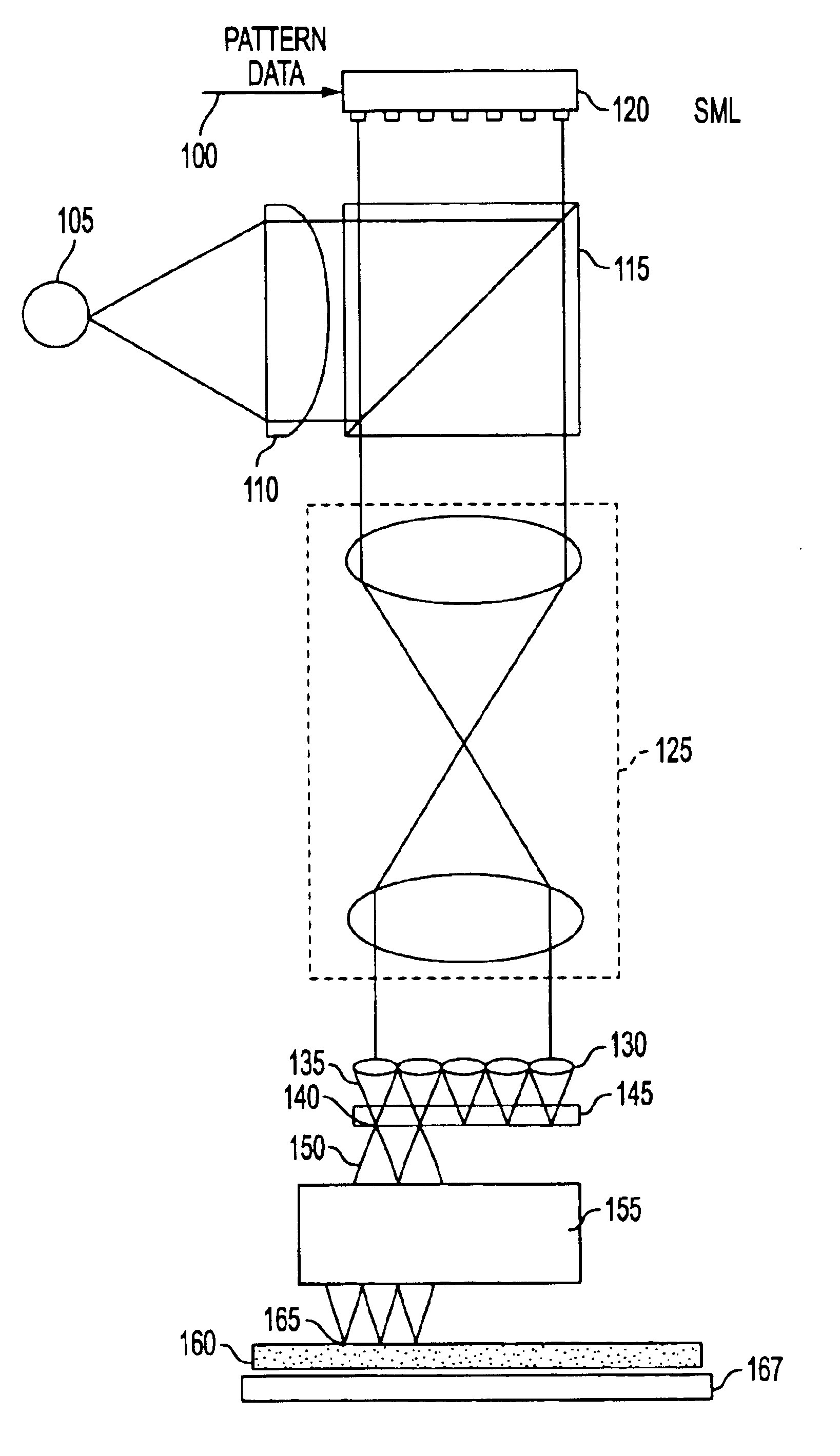
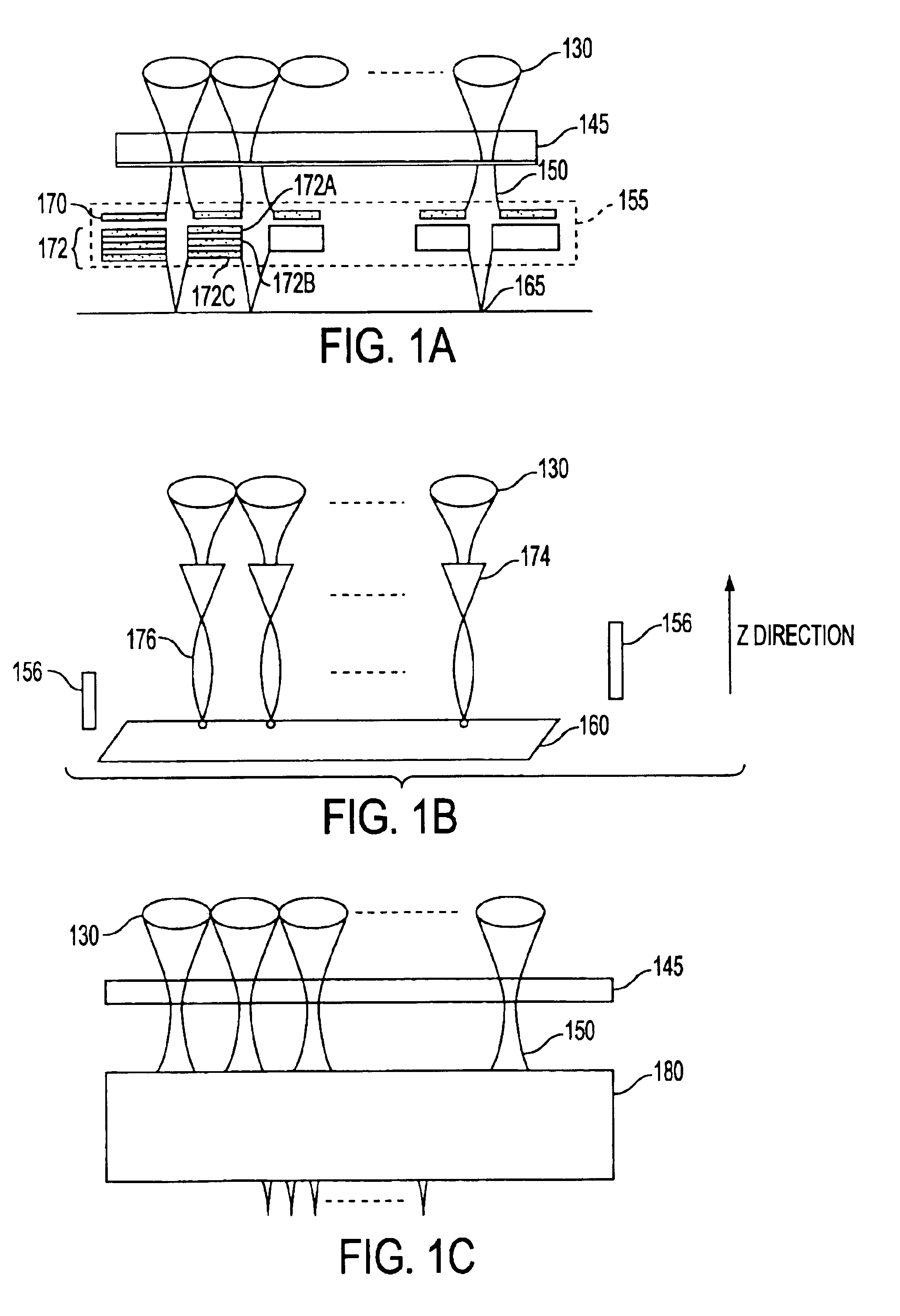
The present invention provides a printer that includes a maskless direct-write hybrid optical / electron imaging system. A programmable optical system forms a massive array of optical beams which are individually focused on a photon-electron converter. The spot-grid pattern formed by the focused optical beams is converted to a corresponding spot-grid pattern of electron beams which are focused on a semiconductor substrate layered with an electron-sensitive resist so as to expose the resist with the spot-grid array pattern. The substrate is then translated relative to the electron beam array by a movable stage as subsequent patterns are focused on the substrate so as to build up a final complete image on the substrate.

In certain embodiments of the present invention, the optical radiation source of the inventive printer includes a light source for generating an array of substantially parallel light beams, and a programmable spatial light modulator selectively modulates optical beams fro...


PUM


Abstract

A high resolution and high data rate spot grid array printer system is provided, wherein an image representative of patterns to be recorded on a reticle or on a layer of a semiconductor die is formed by scanning a substrate with electron beams. Embodiments include a printer comprising an optical radiation source for irradiating a photon-electron converter with a plurality of substantially parallel optical beams, the optical beams being individually modulated to correspond to an image to be recorded on the substrate. The photon-electron converter produces an intermediate image composed of an array of electron beams corresponding to the modulated optical beams. A de-magnifier is interposed between the photon-electron converter and the substrate, for reducing the size of the intermediate image. A movable stage introduces a relative movement between the substrate and the photon-electron converter, such that the substrate is scanned by the electron beams.

Description

FIELD OF THE INVENTIONThe present invention relates to a maskless photon-electron spot-grid array lithography system. The present invention has particular applicability to lithography for imaging semiconductor substrates.BACKGROUND ARTPhotolithography is a technique for producing images on semiconductor devices. Typically, an image formed on a mask or “reticle” is transferred to a semiconductor substrate, or wafer, where it exposes a resist layered on the substrate. It is desired to pattern smaller and smaller features on semiconductor substrates, which requires the use of shorter and shorter wavelengths of the light that is used to image the patterns. Optical lithography systems using light in the deep ultraviolet (UV) wavelengths create patterns with resolutions of about 0.25 microns. Further decreases in wavelength to 193 nm enable the imaging of patterns with resolutions of 0.18 microns and 0.13 microns. For further improvements in resolution even;shorter wavelengths are necessa...

Claims


Application Information

Patent Timeline
IPC IPC(8): G03F7/20H01J37/317G21K5/04H01J37/073H01J37/305H01L21/027
CPCB82Y10/00B82Y40/00G03F7/2057G03F7/70275H01J37/073H01J37/3175H01J37/3177G03F7/70375H01J2237/31779H01J2237/1205G03F7/70291G03F7/70383
Inventor ALMOGY, GILAD
Owner APPLIED MATERIALS INC
Why Eureka
Try Eureka