Method of cleaning a semiconductor processing chamber

a technology of processing chamber and cleaning method, which is applied in the direction of cleaning hollow objects, using liquids, coatings, etc., can solve the problems of reducing wafer throughput, causing residues to build up in the chamber, and cannot be removed by standard dry cleaning processes

Inactive Publication Date: 2005-01-18
APPLIED MATERIALS INC
View PDF42 Cites 160 Cited by
  • Summary
  • Abstract
  • Description
  • Claims
  • Application Information

AI Technical Summary

Benefits of technology

According to one embodiment of the invention, one or more substrates are processed in a substrate processing chamber and the chamber is subsequently cleaned using a dry cleaning process. This substrate processing and dry cleaning sequence is then repeated multiple times before the chamber is further cleaned using an extended cleaning process in which a plasma is formed within the chamber and maintained for at least 5 minutes from an appropriate cleaning gas. In one embodiment, the cleaning gas includes a hydrogen source and a fluorine source. In another embodiment the cleaning gas further includes an oxygen source. In still another embodiment the cleaning gas consists of argon. And in still another embodiment cleaning gas consists of argon and a hydrogen source.

Problems solved by technology

Regardless of whether an in situ or remote cleaning process is employed, over time, residue may build up within the chamber that cannot be removed by standard dry cleaning processes.
This results in a decrease in wafer throughput and a general desire on behalf of the semiconductor manufacturers to use such wet cleaning processes less frequently than dry cleaning processes.

Method used


Image

  • Method of cleaning a semiconductor processing chamber
  • Method of cleaning a semiconductor processing chamber
  • Method of cleaning a semiconductor processing chamber

Examples


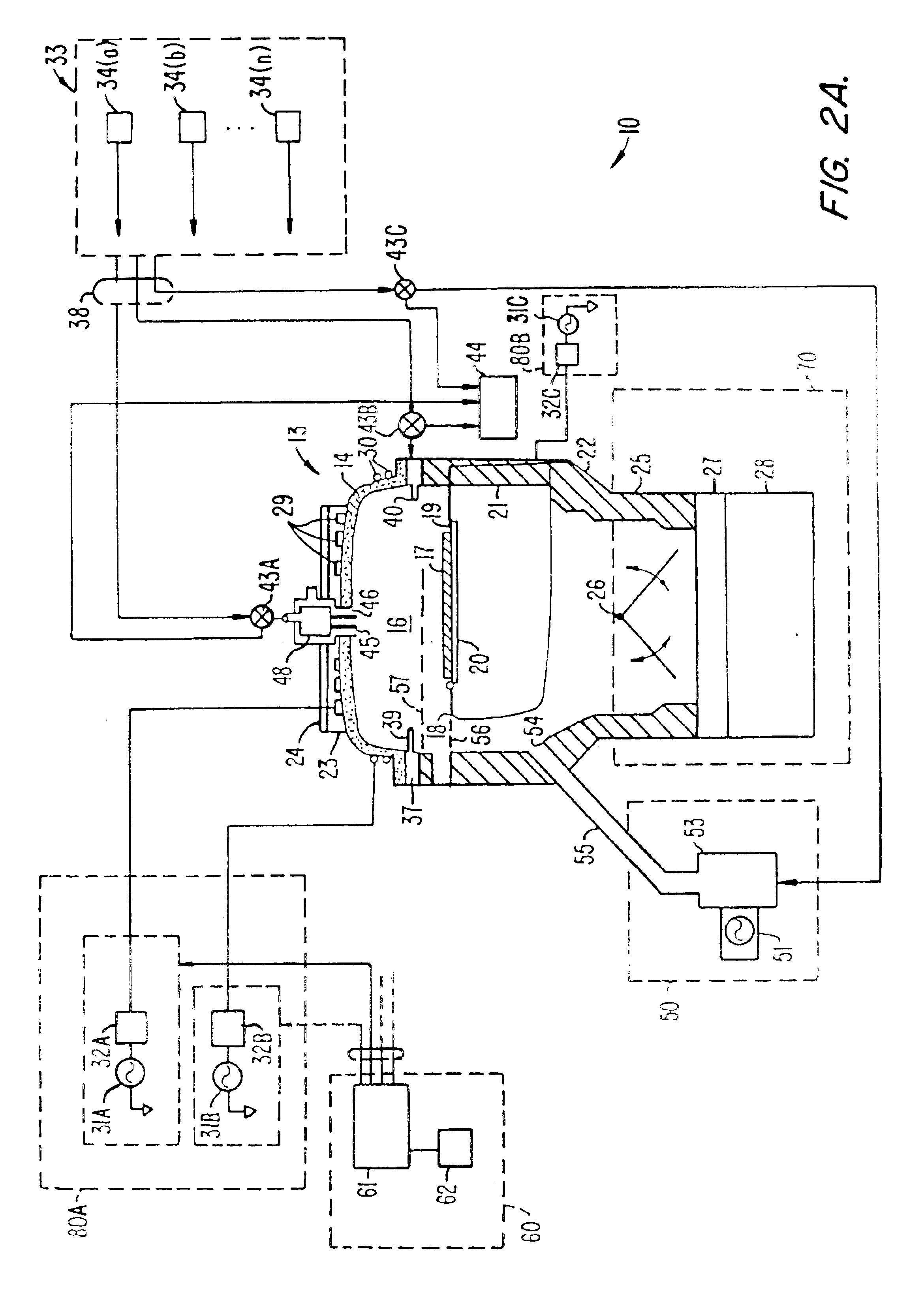
Embodiment Construction

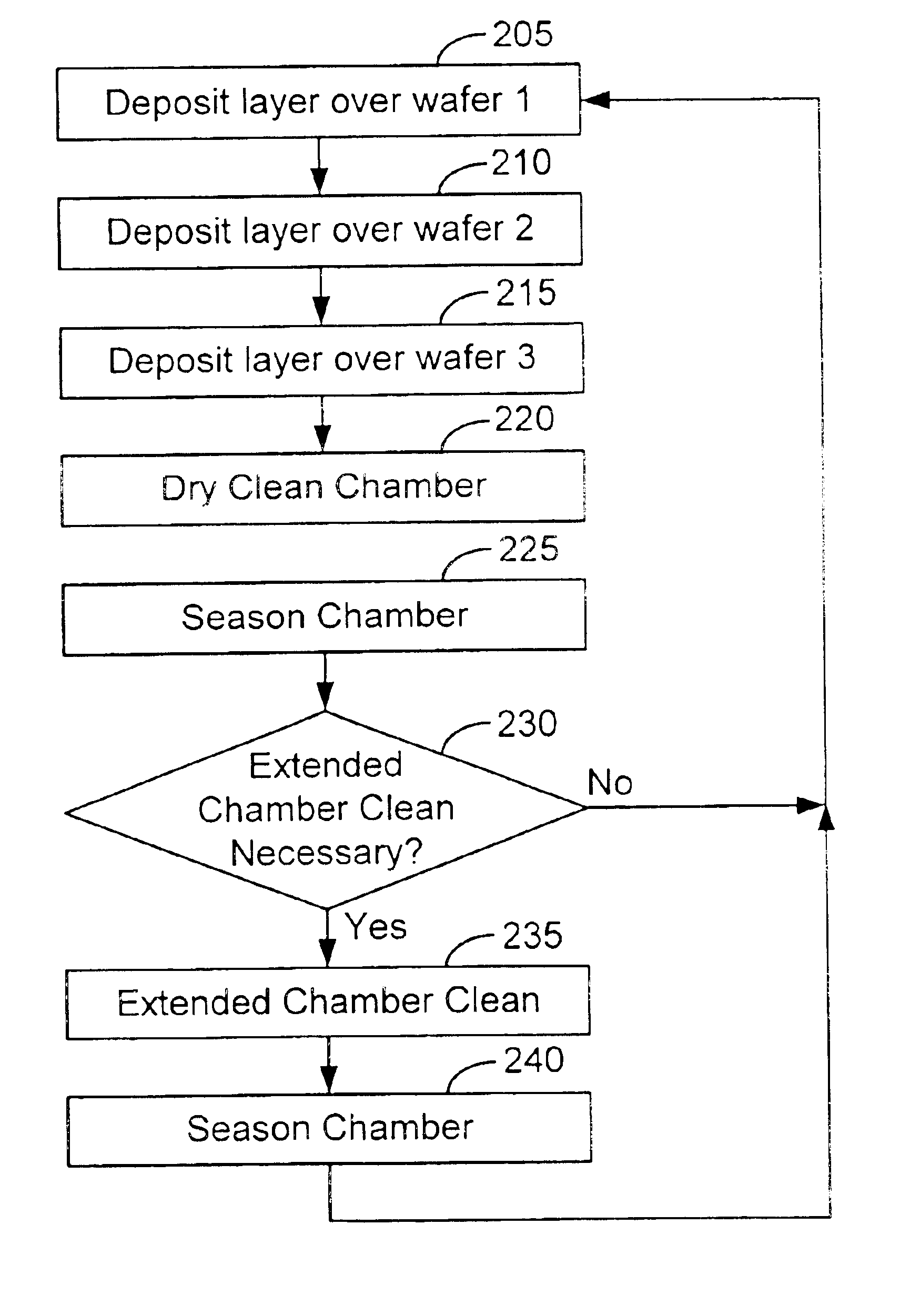
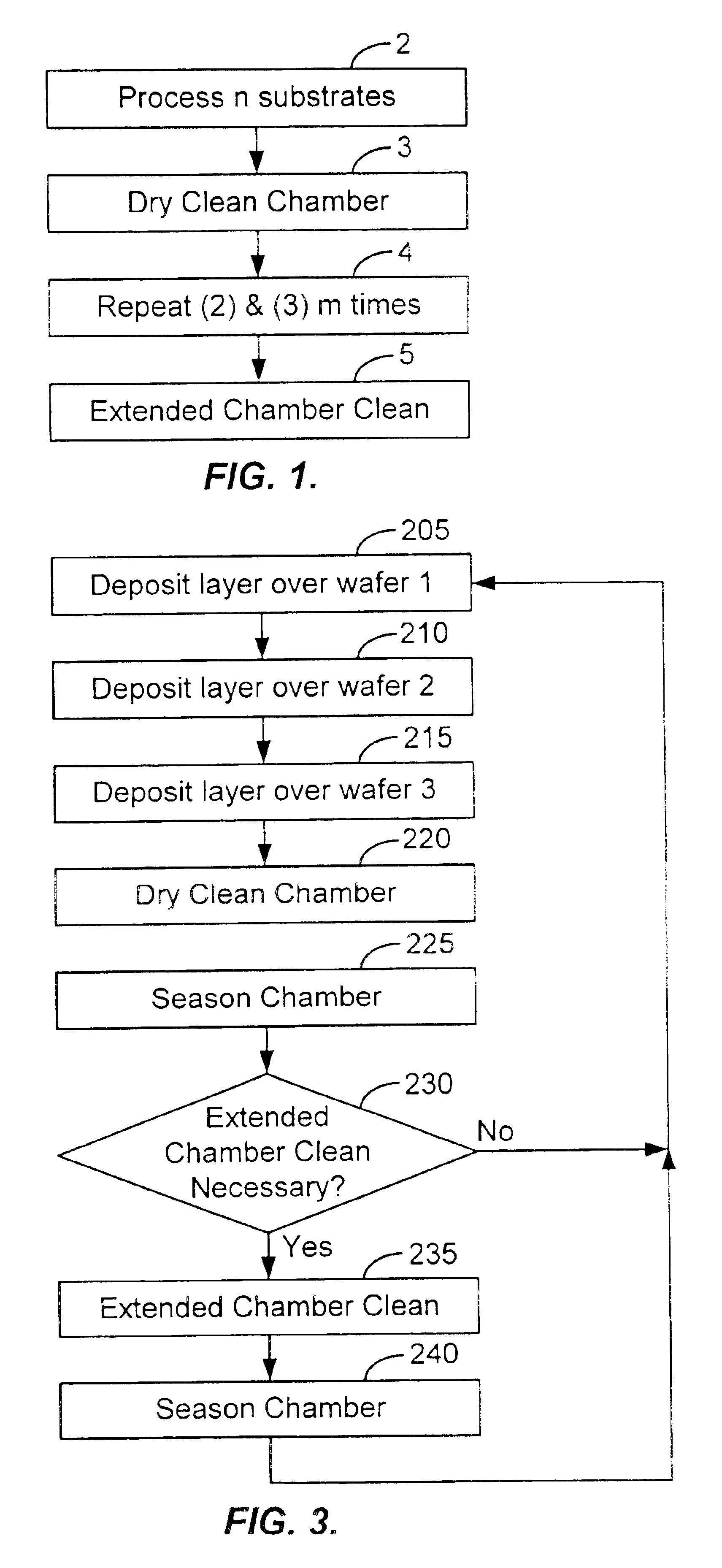
As described above, embodiments of the invention provide a method of removing the residue from a substrate processing chamber that builds up and remains after multiple cycles of substrate processing operations and chamber dry cleaning operations. As used herein a chamber “dry cleaning” operation is any process intended to remove residue from an interior surface of the chamber in the gas phase as opposed to liquid phase. The removal of contaminants in a dry cleaning process is driven by either conversion of the contaminant into a volatile compound through a chemical reaction, by knocking the contaminant off the interior surface via a momentum transfer or by lifting the contaminant off the surface during etching of the surface. Dry cleaning operations include both in situ and remote plasma cleaning processes as well as thermal gas phase cleaning processes and others. Embodiments of the invention are particularly useful in removing residue build-up from a chemical vapor deposition (CVD...


PUM

PropertyMeasurementUnit
pressureaaaaaaaaaa
pressureaaaaaaaaaa
pressureaaaaaaaaaa

Abstract

A method of operating a substrate processing chamber. In one embodiment the method includes processing one or more substrates in the substrate processing chamber and subsequently cleaning the chamber using a dry cleaning process. This substrate processing and dry cleaning sequence is then repeated multiple times before chamber is further cleaned by flowing a cleaning gas into the chamber and forming a plasma within the chamber from the cleaning gas in an extended cleaning process. During the extended cleaning process the plasma is maintained within the chamber for a total of at least 5 minutes before the chamber is reused to process a substrate.

Description

BACKGROUND OF THE INVENTIONThe present invention relates to the fabrication of integrated circuits. More specifically, embodiments of the invention pertain to methods of removing residue from the interior surfaces of a substrate processing chamber.One of the primary steps in the fabrication of modern semiconductor devices is the formation of a layer, such as a silicon oxide layer, on a substrate or wafer. As is well known, such a layer can be deposited by chemical vapor deposition (CVD). In a conventional thermal CVD process, reactive gases are supplied to the substrate surface where heat-induced chemical reactions take place to form the desired film. In a conventional plasma CVD process, a controlled plasma is formed using radio frequency (RF) energy or microwave energy to decompose and / or energize reactive species in reactant gases to produce the desired film.Unwanted deposition on areas such as the walls of the processing chamber also occurs during such CVD processes. As is known...

Claims


Application Information

Patent Timeline
Patent Type & Authority Patents(United States)
IPC IPC(8): B08B7/00C23C16/44
CPCB08B7/0035C23C16/4405Y10S438/905Y10S134/902
Inventor ROSSMAN, KENT
Owner APPLIED MATERIALS INC
Why Eureka
Try Eureka