

Method and apparatus for endpoint detection in electron beam assisted etching
a technology of electron beam and endpoint detection, applied in the direction of individual semiconductor device testing, semiconductor/solid-state device testing/measurement, instruments, etc., can solve the problem that chloride material fails to evaporate well at room temperatur
- Summary
- Abstract
- Description
- Claims
- Application Information
AI Technical Summary
Benefits of technology
Problems solved by technology
Method used
Image

Examples
Embodiment Construction
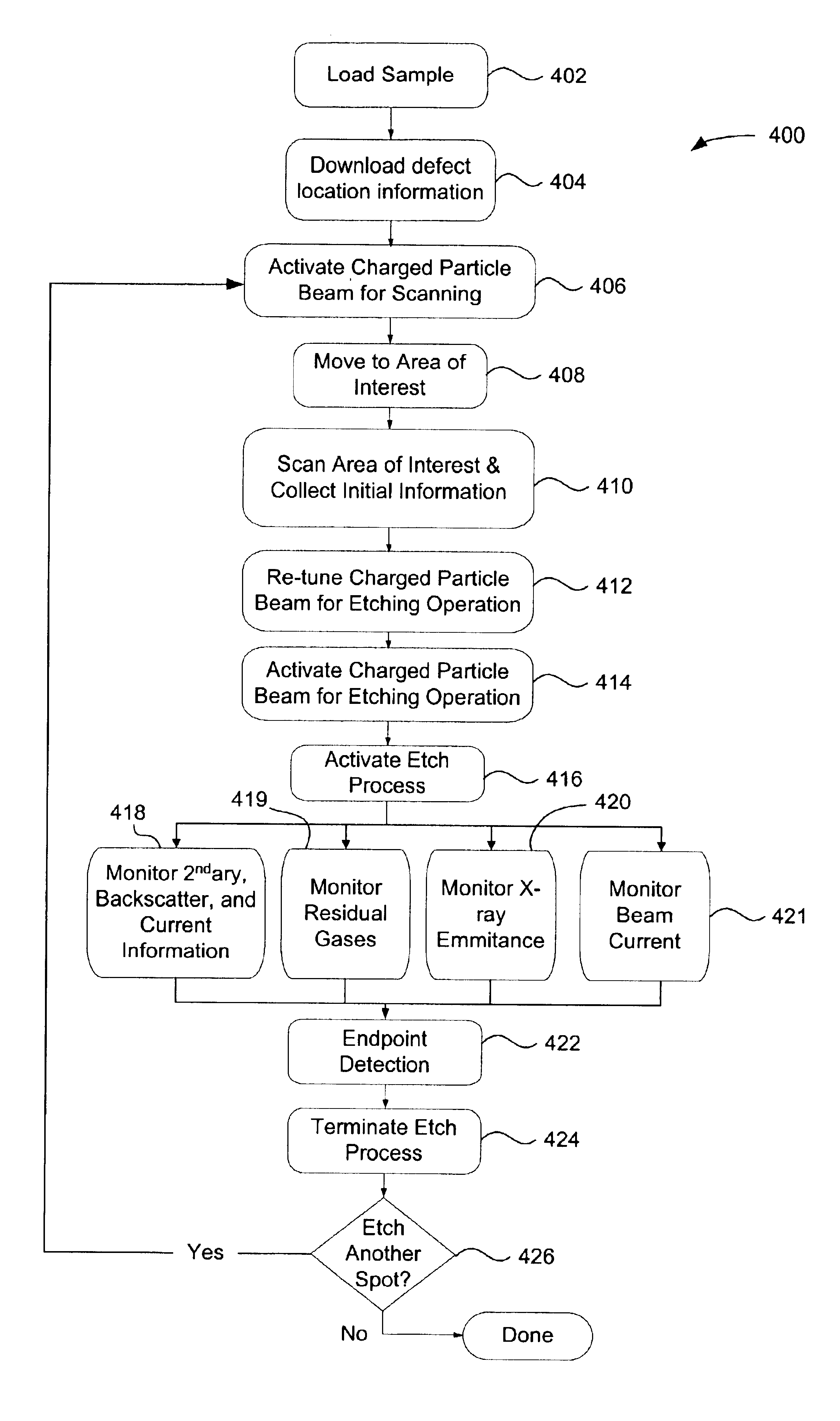
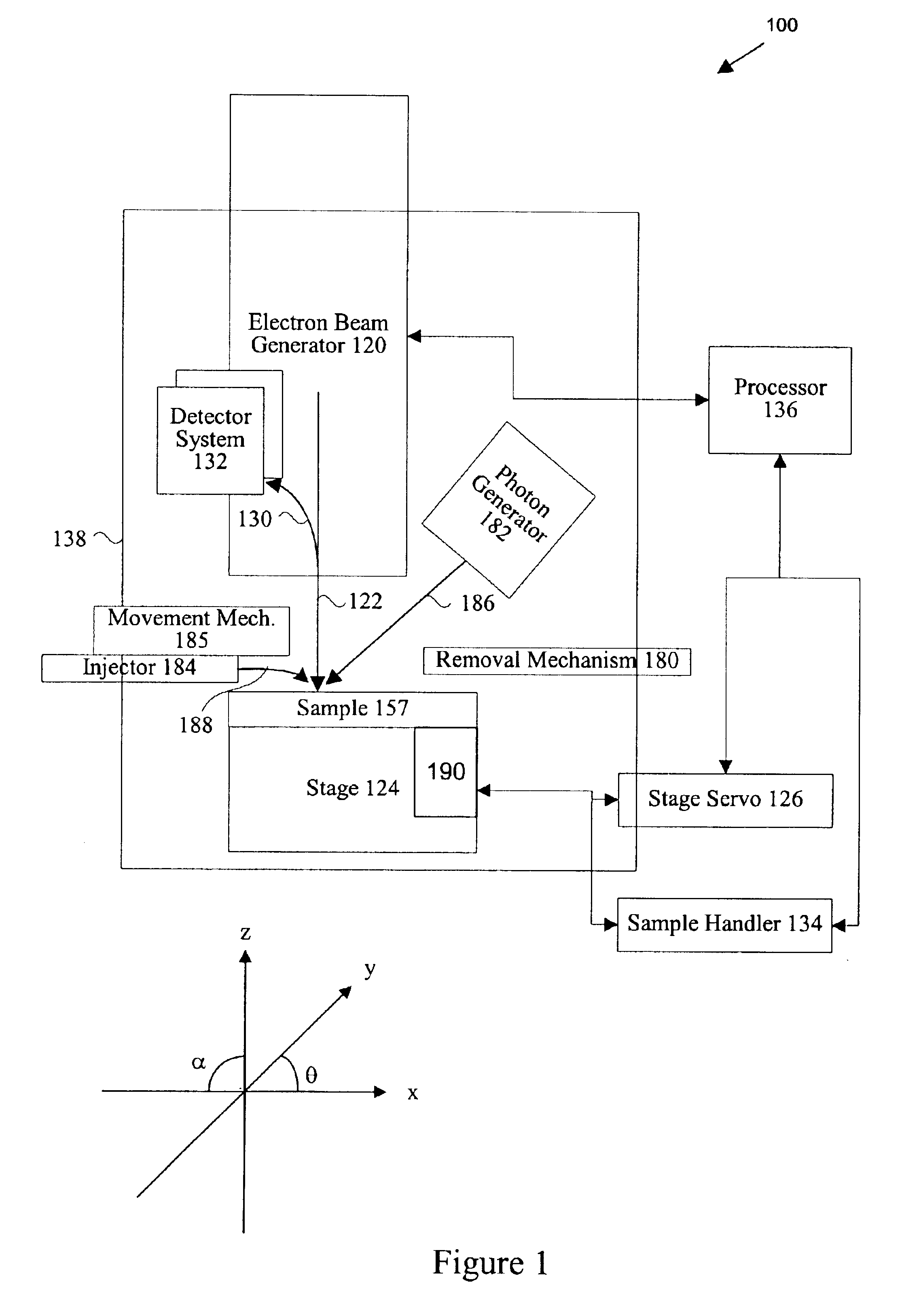
The present invention will now be described in detail with reference to a few preferred embodiments thereof as illustrated in the accompanying drawings. In the following description, numerous specific details are set forth in order to provide a thorough understanding of the present invention. It will be apparent, however, to one skilled in the art, that the present invention may be practiced without some or all of these specific details. In other instances, well known operations have not been described in detail so not to unnecessarily obscure the present invention.
The present invention pertains to techniques for detecting endpoints during semiconductor dry-etching processes. An endpoint refers to a point at which an etch process has reached the boundary (or end) of a layer and therefore the point in time at which the etch process should be terminated. The dry-etching process of the present invention involves using a combination of a reactive material and a an electron beam. In anot...
PUM
| Property | Measurement | Unit |
|---|---|---|
| Fraction | aaaaa | aaaaa |
| Weight | aaaaa | aaaaa |
| Composition | aaaaa | aaaaa |
Abstract
Description
Claims
Application Information