Method for forming shallow well of semiconductor device using low-energy ion implantation

a technology of low-energy ion implantation and semiconductor devices, which is applied in the direction of semiconductor devices, electrical equipment, transistors, etc., can solve the problems of limiting the further reduction of chip sizes and the margin between adjacent wells, and achieve the effect of reducing well resistance and large well margin

Inactive Publication Date: 2005-01-18
SAMSUNG ELECTRONICS CO LTD
View PDF5 Cites 10 Cited by
  • Summary
  • Abstract
  • Description
  • Claims
  • Application Information

AI Technical Summary

Benefits of technology

According to an embodiment of the present invention, a pad nitride layer pattern is formed on a semiconductor substrate, and an isolation trench is formed in the semiconductor substrate by etching the semiconductor substrate using the pad nitride layer pattern as an etch mask. Next, a spacer nitride layer is formed on the inner walls of the trench, and a high-concentration well is formed beneath the trench or at the bottom of the trench by performing low-energy, high-dose ion implantation using the pad nitride layer pattern and the spacer nitride layer as an ion implantation mask. Next, an isolation layer for filling the trench is formed by covering the high-concentration well with an insulating material, planarizing the top surface of the insulating material and removing the pad nitride layer pattern. Subsequently, a low-concentration well is formed to a depth that is partially overlapped with an upper portion of the high-concentration well by performing low-energy ion implantation on the entire surface of the semiconductor substrate. The depth of the entire well including the high-concentration well and the low-concentration well is about the same as the depth of the trench isolation layer, and thus the well may be referred to as a shallow well. In particular, the high-concentration well is formed under the isolation layer. According to the above embodiment, a large margin between adjacent wells can be obtained through vertical down-scaling of the well region, and well resistance can be reduced.
In another embodiment of the present invention, a complementary metal oxide semiconductor (CMOS) well is formed. For this purpose, a pad nitride layer pattern is formed on a semiconductor substrate divided into PMOS and NMOS regions. Next, isolation trenches are formed in the first and second regions by etching the semiconductor substrate using the pad nitride layer pattern as an etch mask. Next, a spacer nitride layer is formed on the inner walls of the trenches. Next, a first photoresist pattern for exposing only the NMOS region is formed, and low-energy, high-dose ion implantation using the pad nitride layer pattern and the spacer nitride layer as an ion implantation mask is performed, thereby forming a P+ well beneath the trench or at the bottom of the trench of the NMOS region. Next, the first photoresist pattern is removed, a second photoresist pattern for exposing only the PMOS region is formed, and low-energy, high-dose ion implantation using the pad nitride layer pattern and the spacer nitride layer as an ion implantation mask is performed, thereby forming an N+ well beneath the trench or at the bottom of the trench of the PMOS region. Next, the second photoresist pattern is removed, the P+ well and the N+ well are covered with an insulating material, the top surface of the insulating material is planarized, and the pad nitride layer pattern is removed, thereby forming an isolation layer for filling the trenches. Next, a third photoresist pattern for exposing only the NMOS region is formed, and low-energy ion implantation the semiconductor substrate is performed, thereby forming a P well to a depth that is partially overlapped with an upper portion of the P+ well. Next, the third photoresist pattern is removed, a fourth photoresist pattern for exposing only the PMOS region is formed, and low-energy ion implantation on the semiconductor substrate is performed, thereby forming an N well to a depth that is partially overlapped with the upper portion of the P+ well. Last, the fourth photoresist pattern is removed. According to the present embodiment, low-energy ion implantation is performed, and thus the first through fourth photoresist patterns can be formed to be thin enough to obtain a large well margin.

Problems solved by technology

However, high-energy ion implantation causes a decrease in a margin between adjacent wells.
This causes a severe deficiency in the margin between adjacent wells, and thus limits the further reduction of chip sizes.
When a well is formed to be shallow using conventional high-energy ion implantation, an increase in resistance causes a malfunction, such as a latch-up, during a device driving operation.

Method used


Image

  • Method for forming shallow well of semiconductor device using low-energy ion implantation
  • Method for forming shallow well of semiconductor device using low-energy ion implantation
  • Method for forming shallow well of semiconductor device using low-energy ion implantation

Examples


Embodiment Construction

The present invention will be described more fully hereinafter with reference to the accompanying drawings in which preferred embodiments of the invention are shown. This invention may, however, be embodied in many different forms and should not be construed as being limited to the embodiments set forth herein. Rather, these embodiments are provided so that this disclosure will be thorough and complete and will fully convey the scope of the invention to those skilled in the art. In the drawings, the forms of elements are exaggerated for clarity. Like reference numerals refer to like elements throughout the drawings.

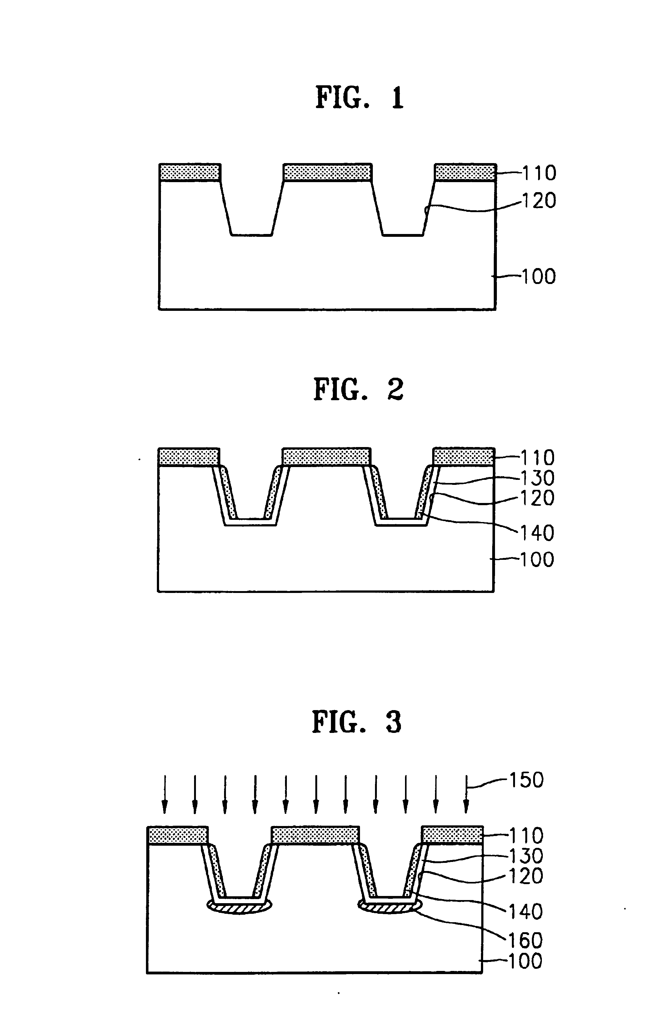
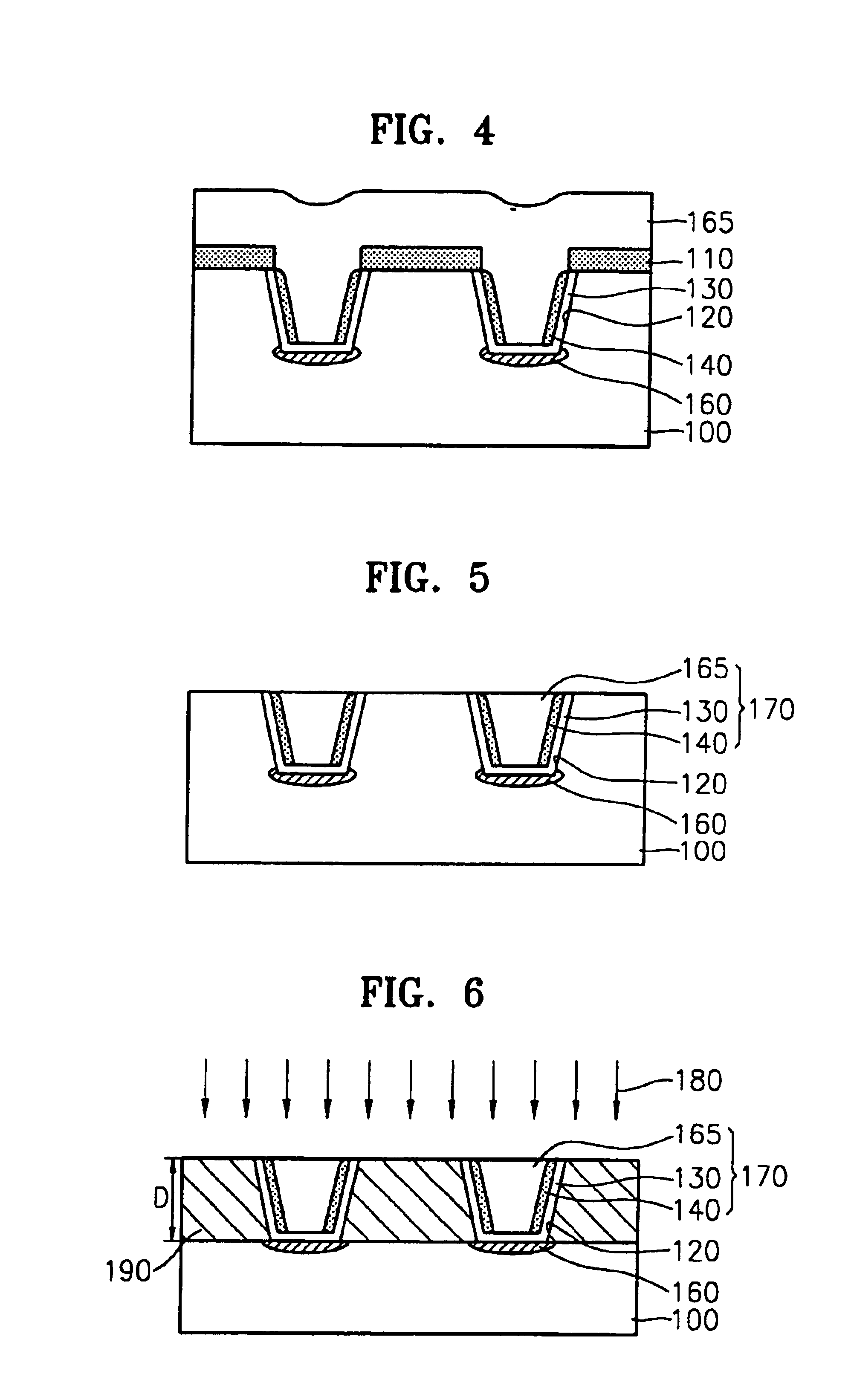
FIGS. 1 through 6 are cross-sectional views illustrating an embodiment of a method for forming a shallow well according to the present invention.

Referring to FIG. 1, a pad nitride layer pattern 110 is formed on a semiconductor substrate 100. Then, the semiconductor substrate 100 is etched to a thickness of about 2500 to about 3000 Å, using the pad nitride layer pattern 11...


PUM


Abstract

A method for forming a shallow well of a semiconductor device using low-energy ion implantation is described. A well region is formed to the depth of a trench isolation layer using a low-energy, high-dose ion implantation process. The method for forming a well using low-energy ion implantation can minimize well margin reduction caused by impurity spread and well margin reduction caused by shrinkage of a thick photoresist pattern.

Description

BACKGROUND OF THE INVENTIONThis application claims priority from Korean Patent Application No. 2002-43698, filed on Jul. 24, 2002, in the Korean Intellectual Property Office, the content of which is incorporated herein by reference in its entirety.1. Field of the InventionThe present invention relates to methods for fabricating semiconductor devices, and more particularly, to methods for forming a well of a highly-integrated semiconductor devices.2. Description of the Related ArtA well of a semiconductor device is used to transfer body voltage to a Metal oxide semiconductor (MOS) device that actually operates and eliminate carriers formed because of impact ionization. In order to allow a well to perform these functions, low resistance should be maintained by implanting a large amount of impurities during a well ion implantation process. In particular, low well resistance plays an important role in testing reliability for such problems as latch-up. Thus, a deep well is formed using h...

Claims


Application Information

Patent Timeline
Patent Type & Authority Patents(United States)
IPC IPC(8): H01L21/762H01L21/70H01L21/8234H01L21/76H01L21/22H01L21/265H01L21/761H01L21/8238H01L21/8242H01L27/08H01L27/092
CPCH01L21/76237H01L27/10844H01L21/823493H01L21/823481H10B12/01H01L21/22
Inventor LEE, JAE-KYU
Owner SAMSUNG ELECTRONICS CO LTD
Why Eureka
Try Eureka