Electrical component and a shuntable/shunted electrical component and method for shunting and deshunting

a technology of electrical components and electrical components, applied in the direction of circuit electrostatic discharge protection, record information storage, instruments, etc., can solve the problems of increasing the risk of damage to electrical components, esd/eos damage the damage to electrical components is a particular problem, so as to reduce or prevent esd/eos damage, the effect of reducing or preventing esd/eos damag

Inactive Publication Date: 2005-01-25
APPLIED KINETICS
View PDF34 Cites 10 Cited by
  • Summary
  • Abstract
  • Description
  • Claims
  • Application Information

AI Technical Summary

Benefits of technology

It is another object of the present invention to provide a method of repeatedly providing and removing electrical shunts to reduce or prevent ESD/EOS damage.
It is s

Problems solved by technology

Damage due to electrostatic discharge (ESD) and/or electrical overstress (EOS) costs industry uncounted and perhaps uncountable dollars daily in damaged and irreparable goods.
More specifically, ESD/EOS damage is a particular problem in the electronics industry where the components are, of course, designed to conduct electricity in the first instance and where their continuously shrinking size renders them increasingly susceptible to such damaging effects.
ESD, familiarly manifested by the lightning bolts or by the shock received when touching a door knob, after walking across a carpet, can range from a few volts to as much as several thousand volts, resulting in extremely large transient currents.
As electronic components shrink in size they become ever more susceptible to damage from smaller and small voltages and current.
That is, if a charged object is brought near an uncharged object, the electric field of the charged object will induce a charge in the object, generating an electric field and potentially a static discharge.
Failing to do so, or failing to provide an avenue for the safe discharge of the accumulated electrostatic charge can result in damage to the MR and GMR heads.
Damage to an MR or GMR head can be manifested as physical damage or magnetic damage.
Magnetic damage can occur in the form of loss of sensing ability and instability.
Damaging current flows in the head can also reportedly be created through electromagnetic interference as a result of a distant (relatively speaking) discharge.
As a result, the individual conductors that make up the electrical interconnect, can easily be charged by stray voltages

Method used


Image

  • Electrical component and a shuntable/shunted electrical component and method for shunting and deshunting
  • Electrical component and a shuntable/shunted electrical component and method for shunting and deshunting
  • Electrical component and a shuntable/shunted electrical component and method for shunting and deshunting

Examples


embodiment 160

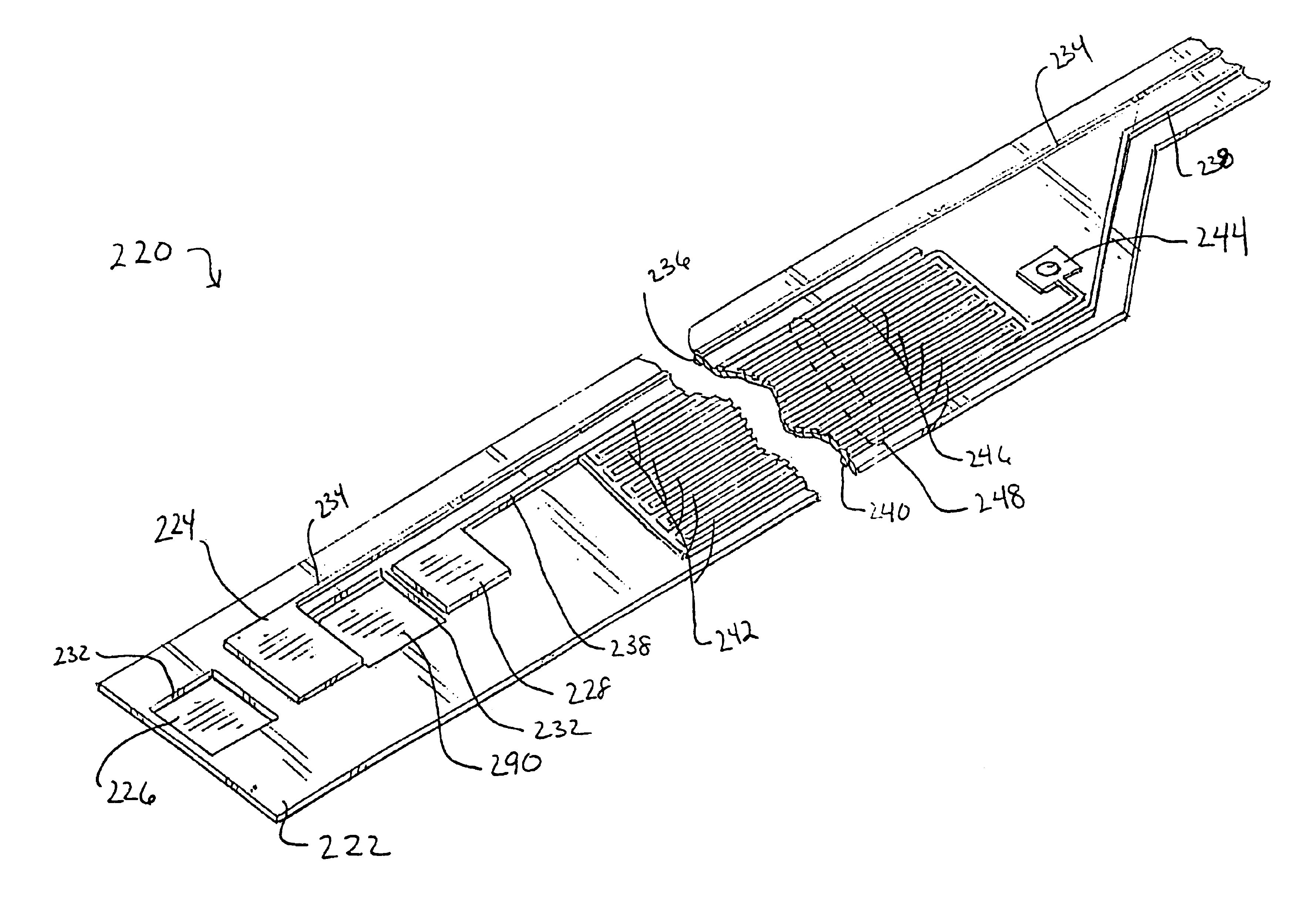
Another embodiment 160 of an interconnect in accord with the present invention is illustrated in FIG. 11. The interconnect 160 includes a substrate 162 that supports a plurality of leads 164. It will be observed that the interconnect 160 includes a terminal end 166 defining a tear-away or shearable portion 168 and an electrical connect portion 170. Terminal end 166 includes a plurality of temporary, tear away or shearable shunt electrical pads 172 and a corresponding plurality of permanent electrical connection pads 174 electrically connected by a similar corresponding plurality of tear-away or shearable leads 176. Like the connection pads 174, the shunt electrical pads 172 are supported upon a substrate that produces a conductive surface area when exposed to a radiant energy source. Thus the surface areas 178 between the shunt pads 172 can be made electrically conductive. The terminal end 166 also includes a through hole 180 underlying the tear-away leads 176. Thus, with this embod...


PUM


Abstract

An interconnect for an electrical component. Generally, interconnects of the invention include a substrate, a pair of leads supported on the substrate, and a shunt extending between the leads. In one aspect of the present invention, the shunt comprises an eroded carbonized area of a surface of a carbonizable material.

Description

FIELD OF THE INVENTIONThe present invention relates generally to methods for eliminating or reducing potential damage to devices from electrostatic discharge or electrical overstress and to such devices, and particularly to methods for reducing such damage to electronic components such as but not limited to a magnetoresistive head forming part of a hard disk drive.BACKGROUND OF THE PRESENT INVENTIONDamage due to electrostatic discharge (ESD) and / or electrical overstress (EOS) costs industry uncounted and perhaps uncountable dollars daily in damaged and irreparable goods. More specifically, ESD / EOS damage is a particular problem in the electronics industry where the components are, of course, designed to conduct electricity in the first instance and where their continuously shrinking size renders them increasingly susceptible to such damaging effects. Generally, ESD refers to actual discharges while EOS refers to the effects of such discharges or currents induced by such discharges o...

Claims


Application Information

Patent Timeline
IPC IPC(8): G11B5/10G11B5/11G11B5/115H05K1/02H05K1/00H05K1/16
CPCG11B5/11G11B5/112G11B5/115H05K1/0259H05K2203/1136H05K1/167H05K2201/0323H05K2203/107H05K1/0393
Inventor GIRARD, MARK T.JURGENSON, RYAN A.
Owner APPLIED KINETICS
Why Eureka
Try Eureka