Semiconductor integrated circuit device

a technology of integrated circuits and semiconductors, applied in the direction of semiconductor devices, electrical equipment, transistors, etc., can solve problems such as acceleration of flow, achieve the effects of reducing leakage currents, and improving the isolating properties of strained substrates

Inactive Publication Date: 2005-01-25
RENESAS ELECTRONICS CORP
View PDF2 Cites 18 Cited by
  • Summary
  • Abstract
  • Description
  • Claims
  • Application Information

AI Technical Summary

Benefits of technology

However, direct filling of the CVD insulating film in the groove accelerates the flow of a leakage current along the groove (walls of the element isolation). This is due to a rise in an interface state density between the CVD insulating film and the semiconductor substrate. Therefore, a method of making a groove and, then, after thermal oxidation of the inside walls thereof, embedding a CVD insulating film in the groove is adopted.
An object of the present invention is to provide a technique that is capable of improving the element isolating properties of a strained substrate, particularly, to reduce the leakage current occurring via the wall of an element isolation, even in the case where a well has a high concentration, or where a conductive film is disposed over the element isolation.
Another object of the present invention is to improve the element isolating properties of a strained substrate, thereby improving the characteristics of the resulting semiconductor integrated circuit formed over the main surface of the substrate and improving the yield of the device.

Problems solved by technology

However, direct filling of the CVD insulating film in the groove accelerates the flow of a leakage current along the groove (walls of the element isolation).

Method used


Image

  • Semiconductor integrated circuit device
  • Semiconductor integrated circuit device
  • Semiconductor integrated circuit device

Examples


embodiment 1

(Embodiment 1)

A semiconductor integrated circuit device according to this Embodiment will be described in the sequence of its manufacturing steps.

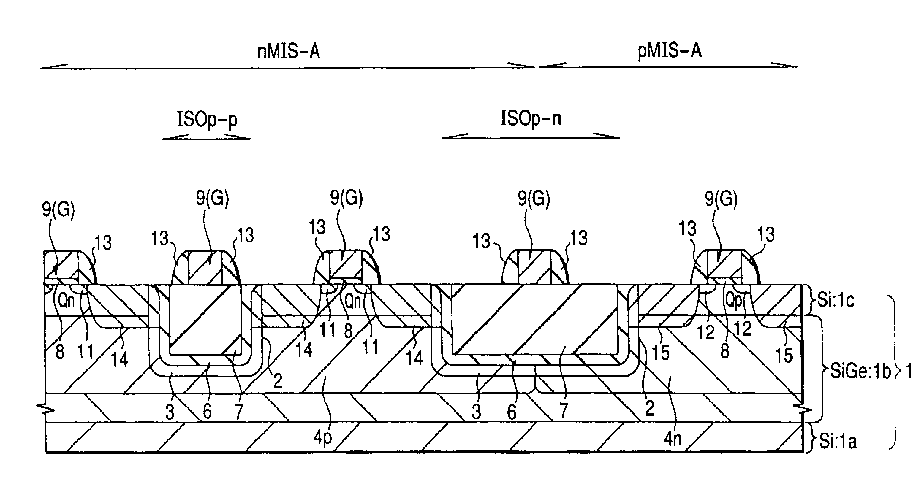
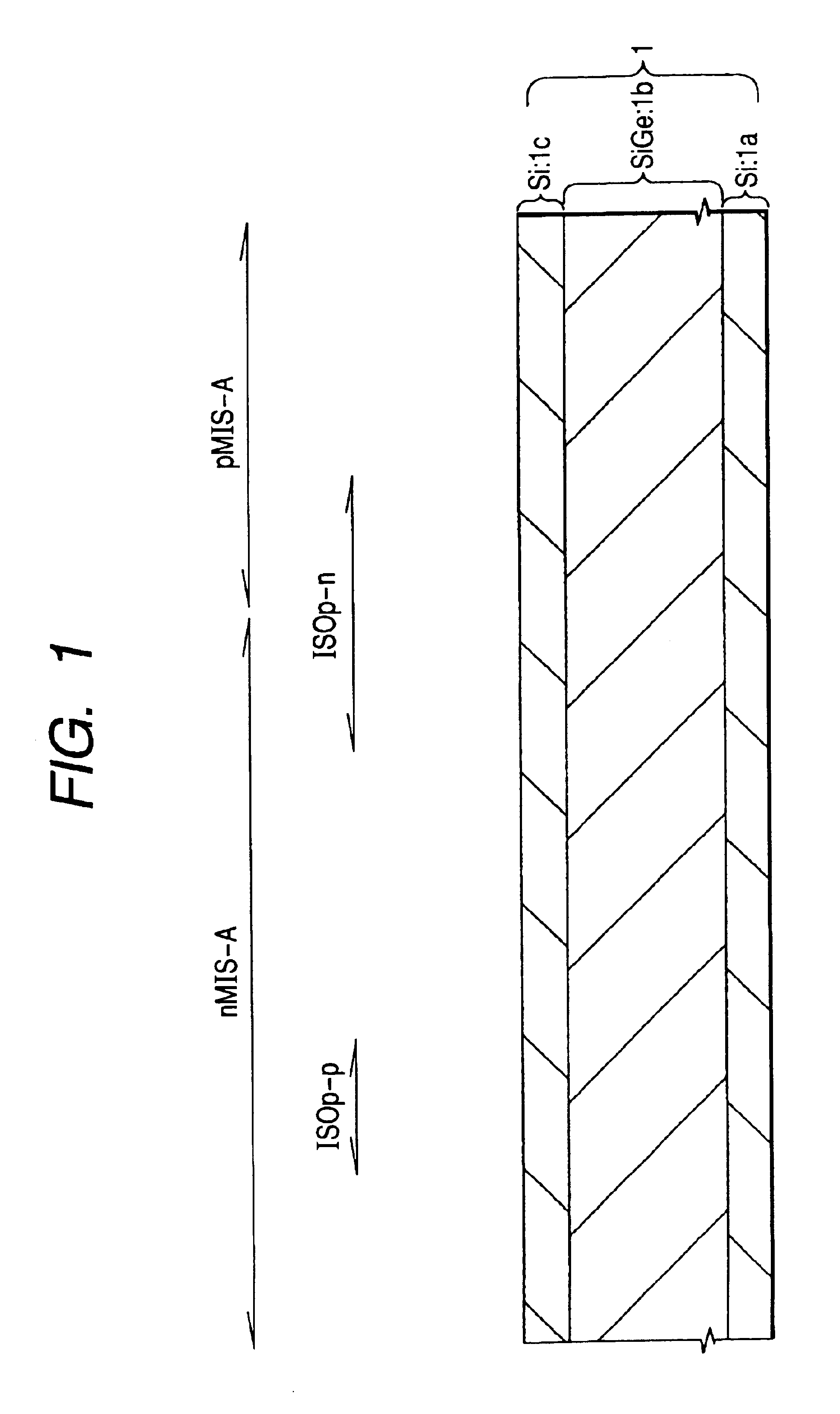
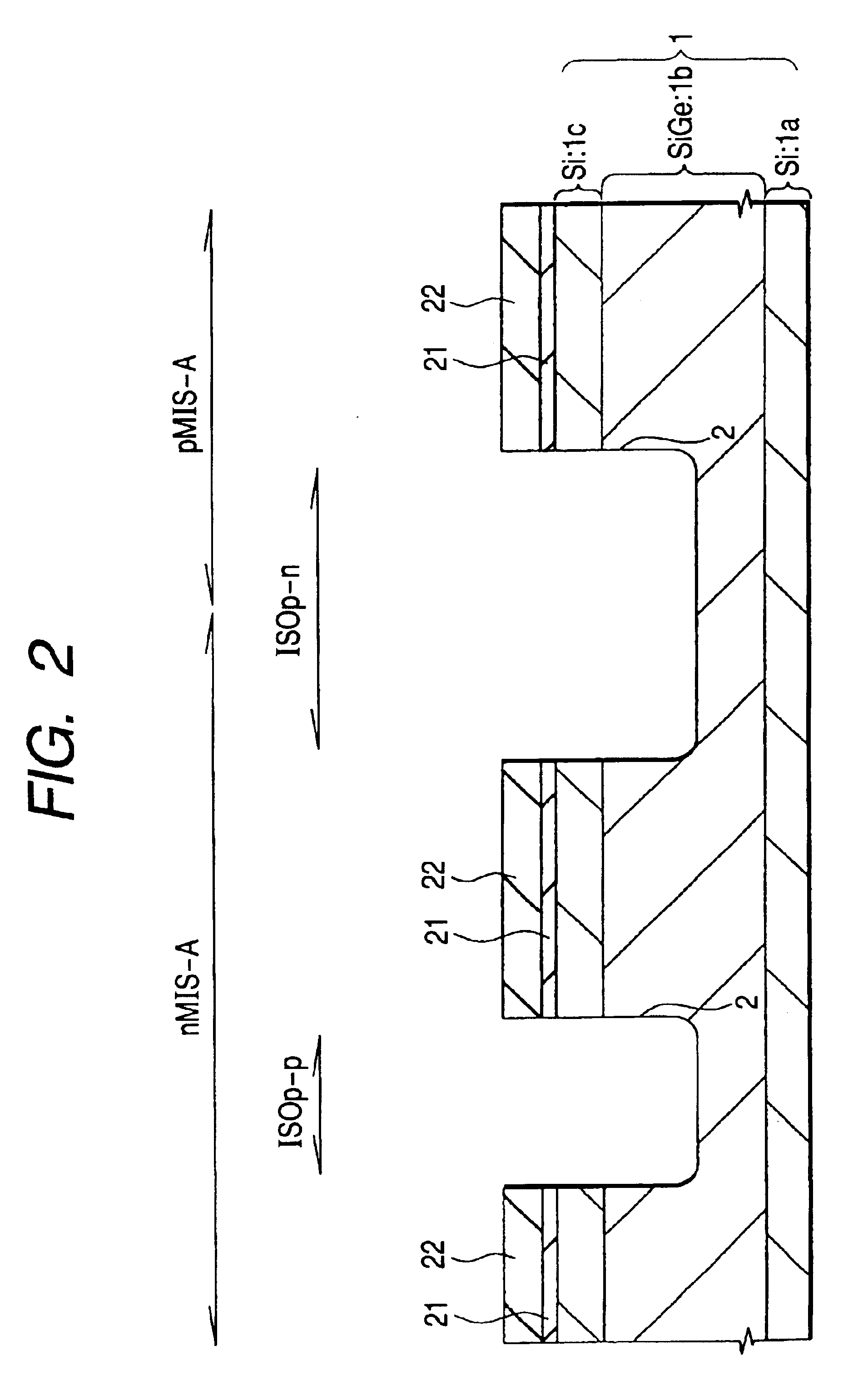
FIGS. 1 to 13 are each a fragmentary cross-sectional view of a substrate illustrating a respective step in the method of manufacture of a semiconductor integrated circuit device according to this Embodiment. FIG. 14 is a fragmentary plan view of the substrate, and each cross-sectional view is a view taken along a line A—A of the plan view. The region nMIS-A is the region where an n-channel type MISFET is formed, while the region pMIS-A is the region where a p-channel type MISFET is formed.

First, a semiconductor substrate (which will hereinafter be called “substrate”, simply) is formed, having, as illustrated in FIG. 1, a single crystal silicon (Si) layer 1a, an SiGe (silicon germanium) layer 1b, and a single crystal Si layer 1c epitaxially grown thereover.

This substrate 1 is formed as follows. First, a SiGe layer 1b of about 5 μm thick is ...

embodiment 2

(Embodiment 2)

In Embodiment 1, a single crystal Si film formed by epitaxial growth is used as the Si film 3. Alternatively, a polycrystalline silicon film is usable.

The semiconductor integrated circuit device of this Embodiment will be described next in the sequence of its manufacturing steps.

FIGS. 20 to 23 are fragmentary cross-sectional views of a substrate, each illustrating the method of manufacture of the semiconductor integrated circuit device according to this Embodiment. Steps up to the formation of the groove 2 are similar to those described in connection with Embodiment 1, based on FIGS. 1 and 2, so that a further description thereof is omitted.

As illustrated in FIG. 20, a polycrystalline silicon film 203 that is about 20 nm thick is deposited by CVD over the strained substrate 1 having the groove 2 formed therein. Numeral 21 indicates a silicon nitride film, while numeral 22 indicates a silicon nitride film.

As illustrated in FIG. 21, the surface of the polycrystalline sil...

embodiment 3

(Embodiment 3)

In Embodiments 1 and 2, the CVD insulating film (7) was deposited directly over the Si oxide film (6 or 206), but it is possible to dispose therebetween a silicon nitride film.

The semiconductor integrated circuit device of this Embodiment will be described next in the sequence of its manufacturing steps. FIGS. 24 to 28 are each a fragmentary cross-sectional view of a substrate illustrating the method of manufacture of the semiconductor integrated circuit device of this Embodiment. Steps up to the formation of the Si oxide film 6 are similar to those of Embodiment 1, as described with reference to FIGS. 1 to 5, so that an explanation of them will be omitted. As described in detail in connection with Embodiment 1 (FIG. 5), the Si oxide film 6 existing at the corner portion (a1) on the bottom of the groove or that existing at the corner portion (a2) at the upper portion of the side walls of the groove are rounded, however this is illustrated in FIG. 24 only simply.

(1) Ove...


PUM


Abstract

A semiconductor integrated circuit device is formed by a semiconductor substrate having an SiGe layer and a first Si layer epitaxially grown thereover, and on which there are element formation regions each partitioned by element isolation regions; a shallow groove isolation, which has a groove formed in each of the element isolation regions and an insulating film inside of the groove, said groove penetrating through the first Si layer and having a bottom in the SiGe layer; a second Si layer formed between the shallow groove isolation and the SiGe layer; and a semiconductor element formed over the main surface of the semiconductor substrate in the element formation regions. This construction enables a reduction in leakage current via the walls of the shallow groove isolation of the strained substrate, thereby improving the element isolation properties.

Description

BACKGROUND OF THE INVENTIONThe present invention relates to a semiconductor integrated circuit device and to a method of manufacture thereof; and, more particularly, the invention relates to a technique that is effective when applied to a semiconductor integrated circuit device using a so-called strained substrate, which is a substrate to which a stress has been applied at a surface portion thereof, and to a method of manufacture of the device.Characteristics of a semiconductor element, such as a MISFET (Metal Insulator Semiconductor Field Effect Transistor), that is formed over the main surface of a semiconductor substrate are determined by various factors. When a tensile stress is applied to the surface layer of the substrate, the mobility of electrons in a channel region increases, which improves the current driving capacity of the MISFET.Such a substrate is called a “strained substrate”. A description of a MOSFET using such a substrate can be found, for example, in Strained Si M...

Claims


Application Information

Patent Timeline
Patent Type & Authority Patents(United States)
IPC IPC(8): H01L21/762H01L21/70H01L21/8238H01L21/76H01L27/08H01L27/092H01L29/78
CPCH01L21/76224H01L21/823878H01L21/76229H01L29/78
Inventor ICHINOSE, KATSUHIKOOOTSUKA, FUMIO
Owner RENESAS ELECTRONICS CORP
Why Eureka
Try Eureka