Electron beam apparatus and image forming apparatus

a technology of electron beam and image forming apparatus, which is applied in the manufacture of electric discharge tubes/lamps, discharge tubes with screens, discharge tubes luminescnet screens, etc., can solve the problems of difficult heat melting of substrates and inability to faithfully express the position, so as to facilitate the manufacture and facilitate the control of electric conductivity. , the effect of resisting

Inactive Publication Date: 2005-01-25
CANON KK
View PDF19 Cites 12 Cited by
  • Summary
  • Abstract
  • Description
  • Claims
  • Application Information

AI Technical Summary

Benefits of technology

If the average particle diameter is set equal to or less than 1000 Å, the deviation of the fine particles, or the deviation of the secondary particles due to the coagulated fine particles may be suppressed. Also, the electric characteristic of the layer including the fine particles is stabilized. In particular, in the case of using a binder, the degree of dispersion of the fine particles within the binder is readily controlled. If the fine particles include metal elements, the electric conductivity (resistance) can be stabilized. The metal elements may be made into a compound with other elements and may preferably form metal oxide or metal nitride. The average particle diameter may be set equal to or less than 200 Å, or more preferably equal to or less than 100 Å.
In the above invention, the layer including the above fine particles may be disposed on a base substance that constitutes the above spacer. It is not necessary to expose the layer including the fine particles from the surface of the spacer, and another layer may be further disposed on the layer including the fine particles. In this case, the sheet resistance includes contributions of the resistance of the layer including the fine particles and the resistance of another layer. The use of the base substance of the spacer facilitates the manufacture and also facilitates the control of the electric conductivity (resistance). It is preferable that the base substance of the spacer is made of insulating material. Further, it is unnecessary that the region that satisfies the above conditions of the present invention exists on the entire surface of the spacer.

Problems solved by technology

However, this shape is schematic and does not faithfully express the position and the configuration of the actual electron emission portion.
Also, in the cold cathode element, even if a large number of elements are disposed on the substrate with a high density, a problem such as heat melting of the substrate is difficult to occur.

Method used


Image

  • Electron beam apparatus and image forming apparatus
  • Electron beam apparatus and image forming apparatus
  • Electron beam apparatus and image forming apparatus

Examples


embodiment 1

[Embodiment 1]

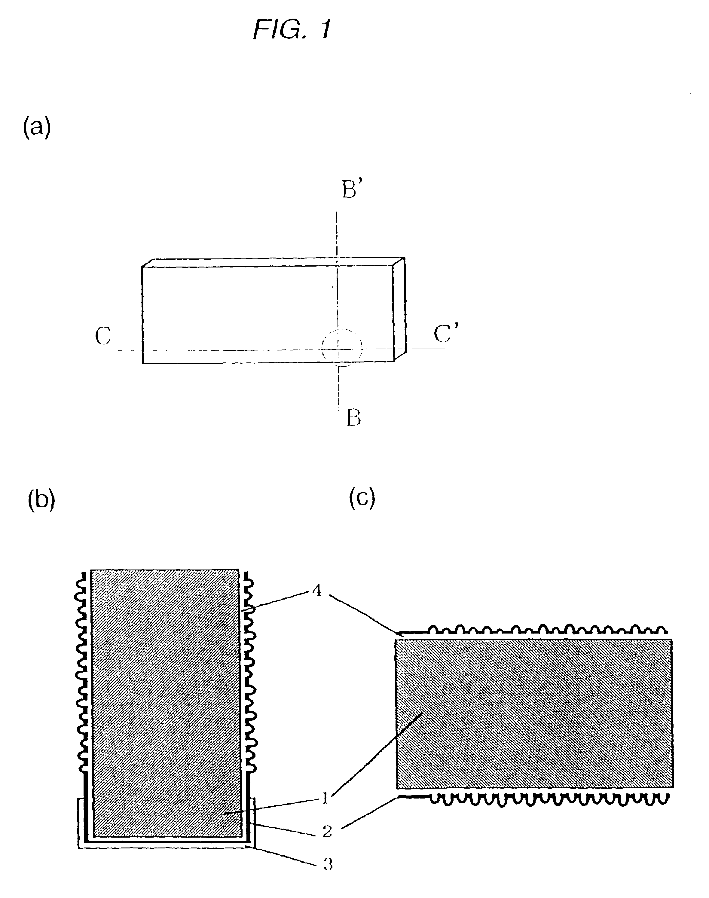
A spacer used in this embodiment was produced as follows:

A ceramic substrate into which zirconia and alumina were mixed with each other at the weight ratio of 65:35 so as to provide the same coefficient of thermal expansion as that of the soda lime glass substrate which was the same in quality as the rear plate was subjected to a grinding process so that its outer dimensions became 0.2 mm in thickness, 3 mm in height and 40 mm in length. The average value of the roughness of the surface was 100 [Å]. The substrate will be referred to as a0.

First, prior to a film forming process, after the above spacer substrate a0 was cleaned by ultrasonic waves in pure water, IPA and acetone for 3 minutes, and then dried at 80° C. for 30 minutes, it was subjected to UV ozone cleaning to remove the organic remaining material on the substrate surface.

In addition, fine particles of silica 1000 Å in average diameter of the particles (900 to 1100 Å in the distribution of 3σ) were previously...

embodiment 2

[Embodiment 2]

The following glass substrate g0 was used as a spacer substrate, and a spacer having the concave and convex surface was manufactured in the same manner as that in the Embodiment 1.

As a low alkali glass substrate which was the same in quality as the rear plate, a prototype of PD200 made by Asahi Glass Corp., was subjected to a cutting process and a mirror grinding process so that its outer dimensions became 0.2 mm in thickness, 3 mm in height and 40 mm in length. The average value of the roughness of the surface at this time was 50 [Å]. The substrate will be referred to as g0. First, prior to a film forming process, after the above spacer substrate g0 was cleaned by ultrasonic waves in pure water, IPA and acetone for 3 minutes, and then dried at 80° C. for 30 minutes, it was subjected to UV ozone cleaning to remove the organic remaining material on the substrate surface.

In addition, as in Embodiment 1, fine particles of silica 650 Å in average diameter of the particles ...

embodiment 3

[Embodiment 3]

The glass substrate g0 employed in the Embodiment 2 was used as a spacer substrate, and a spacer having the concave and convex surface was manufactured in the same manner as that in the Embodiment 1.

As in the Embodiment 1, first, prior to a film forming process, after the above spacer substrate g0 was cleaned by ultrasonic waves in pure water, IPA and acetone for 3 minutes, and then dried at 80° C. for 30 minutes, it was subjected to UV ozone cleaning to remove the organic remaining material on the substrate surface.

In addition, as in the Embodiment 1, fine particles of silica 650 Å in average diameter of the particles (500 to 800 Å in the distribution of 3σ) and tin oxide particles 50 Å in average diameter of the particles for enhancing the adhesion were previously dispersed in a metal alkoxide solution of 12.0 weight % containing the component of Ti:Si with the ratio of 1:1, and printing in the solution was conducted by using a solution extended plate 5 μm in roughne...


PUM


Abstract

The present invention is concerned with an electron beam apparatus comprising: a hermetic container; an electron source disposed within the hermetic container; and a spacer; wherein the spacer includes at least a region where a layer containing fine particles exists, a sheet resistance measured at the surface of the region of the spacer is 107 Ω / □ or more, and the fine particles are 1000 Å or less in the average diameter of the particles and includes at least metal elements. The electron beam apparatus exhibits the excellent display quality which suppresses the displacement of the light emission point with the charge and the creeping discharge, and the long-period reliability.

Description

BACKGROUND OF THE INVENTION1. Field of the InventionTECHNICAL FIELDThe present invention relates to an electron beam apparatus and an image forming apparatus, particularly to an electron beam apparatus and an image forming apparatus having a spacer, and more particularly to an electron beam apparatus and an image forming apparatus having an antistatic film.2. Background ArtUp to now, as the electron emitting elements, there have been known a hot cathode element and a cold cathode element. As the cold cathode element of those elements, there have been known, for example, a surface conduction type electron emission element, a field emission element (hereinafter referred to as “FE type”), a metal / insulating layer / metal type emission element (hereinafter referred to as “MIM type”), etc.As the surface conduction type electron emission elements, there have been known, for example, an example disclosed in Radio Eng. Electron Phys., 10, 1290 (1965) by M. I. Elinson, or other examples which ...

Claims


Application Information

Patent Timeline
Patent Type & Authority Patents(United States)
IPC IPC(8): H01J29/02H01J29/86H01J31/12
CPCH01J29/028H01J29/864H01J31/123H01J31/127H01J2329/8625H01J2329/866H01J2329/8635H01J2329/864H01J2329/8645H01J2329/8655H01J2329/863H01J31/12
Inventor ITO, NOBUHIRO
Owner CANON KK
Why Eureka
Try Eureka