

Semiconductor device equipped with transfer circuit for cascade connection
a technology of cascade connection and transfer circuit, which is applied in the direction of digital computers, digital storage, instruments, etc., can solve the problems of increasing the cost of printed boards, difficulty in timing adjustment, and insignificant crosstalk noise between signal lines, so as to reduce timing differences and reduce the crosstalk effect in signal transfer sections
- Summary
- Abstract
- Description
- Claims
- Application Information
AI Technical Summary
Benefits of technology
Problems solved by technology
Method used
Image

Examples
first embodiment
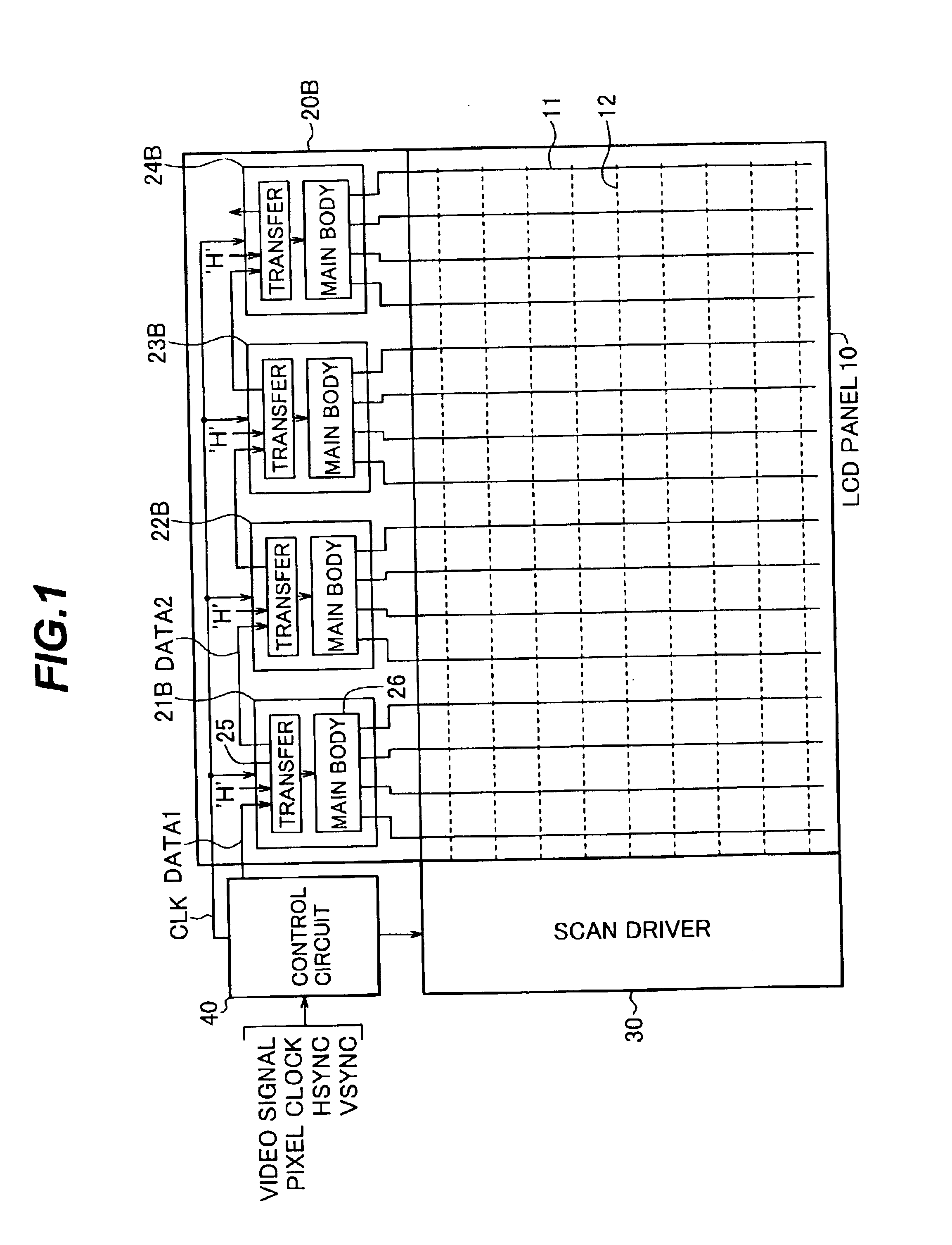
FIG. 1 is a schematic block diagram showing a liquid crystal display device according to a first embodiment of the present invention.
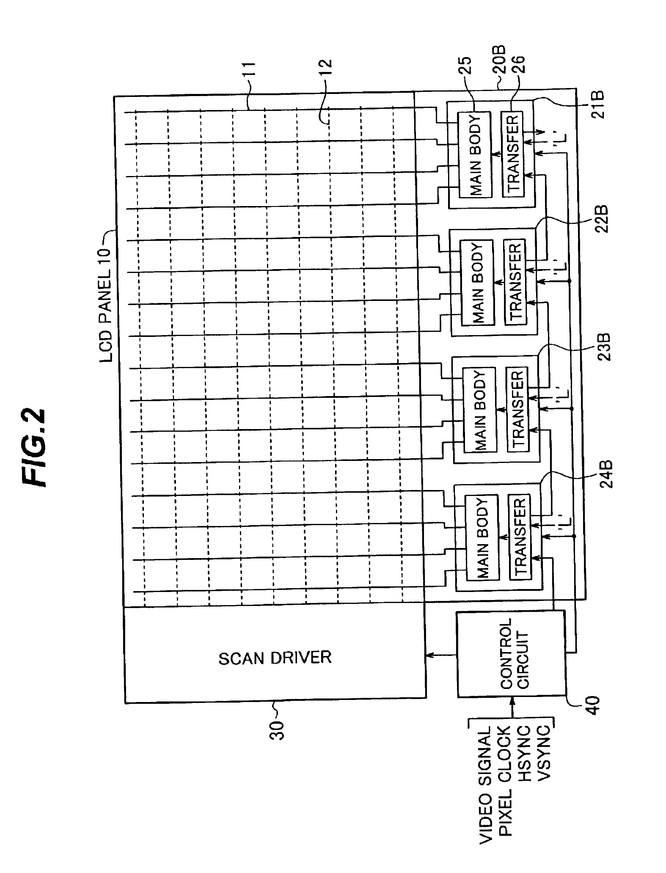
In an LCD panel 10, a plurality of vertically extended data lines 11 and a plurality of horizontally extended scan lines 12 are formed crossing over each other, and a pixel is formed at each crossover point. One ends of the data lines 11 and the scan lines 12 are connected to a data driver 20B and a scan driver 30, respectively. Based on a video signal, a pixel clock signal, a horizontal synchronizing signal, and a vertical synchronizing signal provided from the external, a control circuit 40 provides a data signal DATA1 and a clock signal CLK to the data driver 20B, and also provides a scan control signal to the scan driver 30.
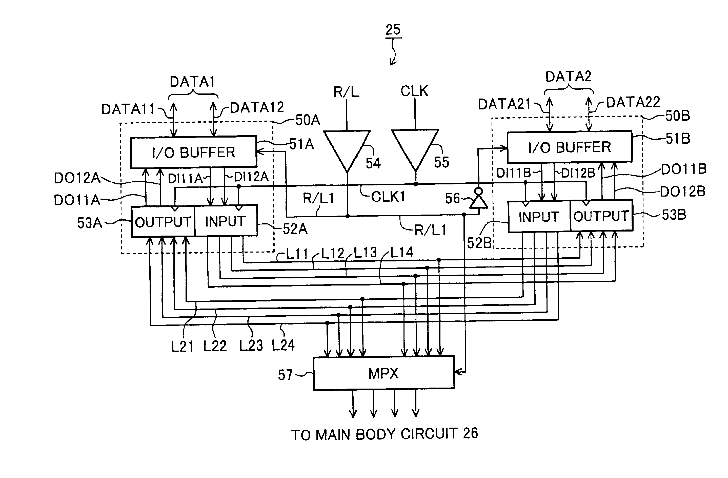
The data driver 20B includes data driver ICs 21B to 24B having the same configuration. The data driver IC 21B includes a transfer circuit 25 and a main body circuit 26, both operating in synchronism with the clock signal CLK. Th...
second embodiment
FIG. 7 is a block diagram showing a transfer circuit 25A according to a second embodiment of the present invention.
In this circuit, the input circuits 52A and 52B of FIG. 3 are omitted by connecting an input circuit 52 to the output of a multiplexer 57A. The input circuit 52 has the same structure as the input circuit 52A of FIG. 3.
The multiplexer 57A selects external input data signals DI11A and DI12A provided from the I / O buffer circuit 51A when the transfer direction control signal R / L is ‘H’, and external input data signals DI11B and DI12B provided from the I / O buffer circuit 51B when R / L is ‘L’, and then provides the selected signals to the input circuit 52.
The outputs of the input circuit 52 are connected to first ends of the signal lines L31 to L34, and second and third ends of the signal lines L31 to L34 are connected to the inputs of the output circuits 53A and 53B, respectively.
When the transfer direction control signal R / L is ‘H’, the data signal DATA1 is provided through...
third embodiment
FIG. 8 is a block diagram showing a transfer circuit 25B according to a third embodiment of the present invention.
In this circuit, the output circuits 53A and 53B of FIG. 7 are omitted by disposing an output circuit 53 on the side of the input circuit 52. The output circuit 53 has the same structure as the output circuit 53A of FIG. 7. The Input of the output circuit 53 is connected to the output of the input circuit 52, the output of the output circuit 53 is connected to first ends of signal lines L41 and L42, and second and third ends of the signal lines L41 and L42 are connected, respectively, to the inputs of the IO buffer circuits 51A and 51B.
According to the third embodiment, it is possible to make the number of data signal lines smaller than the first and second embodiments, and thereby ground lines GND as shown in FIG. 9 can be easily formed at intervals between the data lines extendedly disposed between the I / O buffer circuits 51A and 51B, which allows the crosstalk effect ...
PUM
| Property | Measurement | Unit |
|---|---|---|
| frequency | aaaaa | aaaaa |
| distance | aaaaa | aaaaa |
| delay time | aaaaa | aaaaa |
Abstract
Description
Claims
Application Information