Polishing pad for electrochemical mechanical polishing

a technology of mechanical polishing and polishing pads, which is applied in the direction of electrolysis components, manufacturing tools, lapping machines, etc., can solve the problems of affecting the mechanical aspect of cmp is reaching the limit of its ability to planarize such ic substrates, and the delamination and fracture of the underlayer cap and dielectric materials. to achieve the effect of facilitating the flow of polishing fluid

Inactive Publication Date: 2005-02-01
ROHM & HAAS ELECTRONICS MATERIALS CMP HLDG INC
View PDF15 Cites 95 Cited by
  • Summary
  • Abstract
  • Description
  • Claims
  • Application Information

AI Technical Summary

Benefits of technology

[0014]In a first aspect, the present invention is directed to a polishing pad for electrochemical mechanical polishing of a conductive substrate, said pad comprising: a plurality of grooves formed in a polishing surface of the polishin

Problems solved by technology

Such insulators tend to be less mechanically robust than conventional dielectric materials.
Unfortunately, the mechanical aspect of CMP is reaching the limit of its ability to planarize such IC substrates because the layers cannot handle the mechanical stress of polishing.
In particular, delamination and fracture of the underlayer cap and dielectric material occur during CM

Method used


Image

  • Polishing pad for electrochemical mechanical polishing
  • Polishing pad for electrochemical mechanical polishing
  • Polishing pad for electrochemical mechanical polishing

Examples


Embodiment Construction

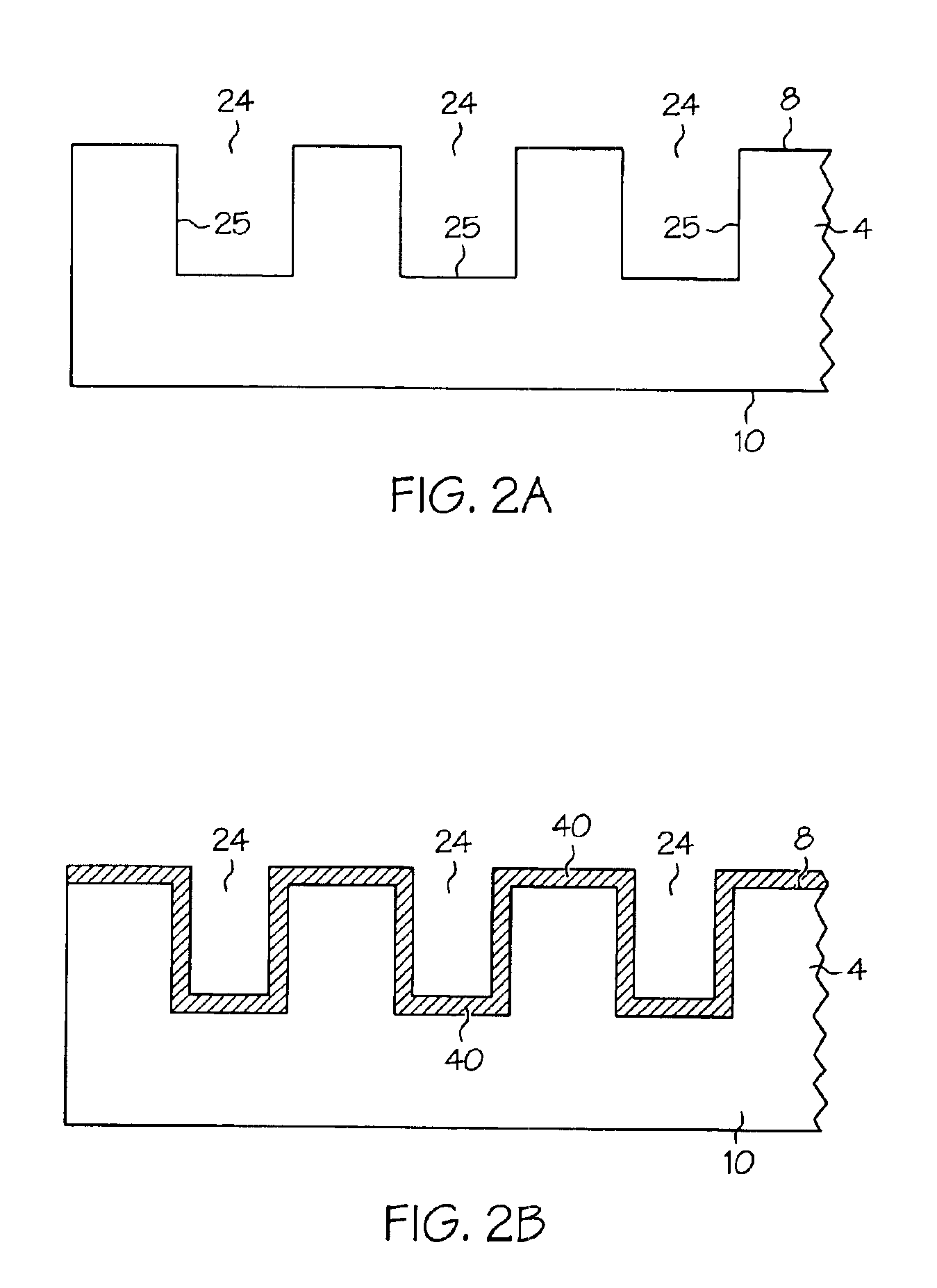
rein the polishing pad comprises: a plurality of grooves formed in a polishing surface of the polishing pad, the grooves being adapted to facilitate flow of the polishing fluid over the polishing pad; conductive layers respectively formed in the grooves; and wherein the conductive layers are in electrical communication with each other.

DETAILED DESCRIPTION OF THE INVENTION

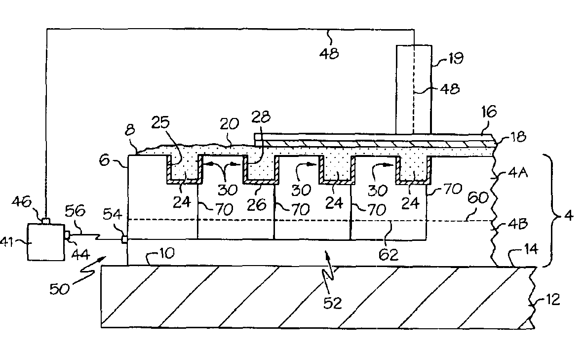
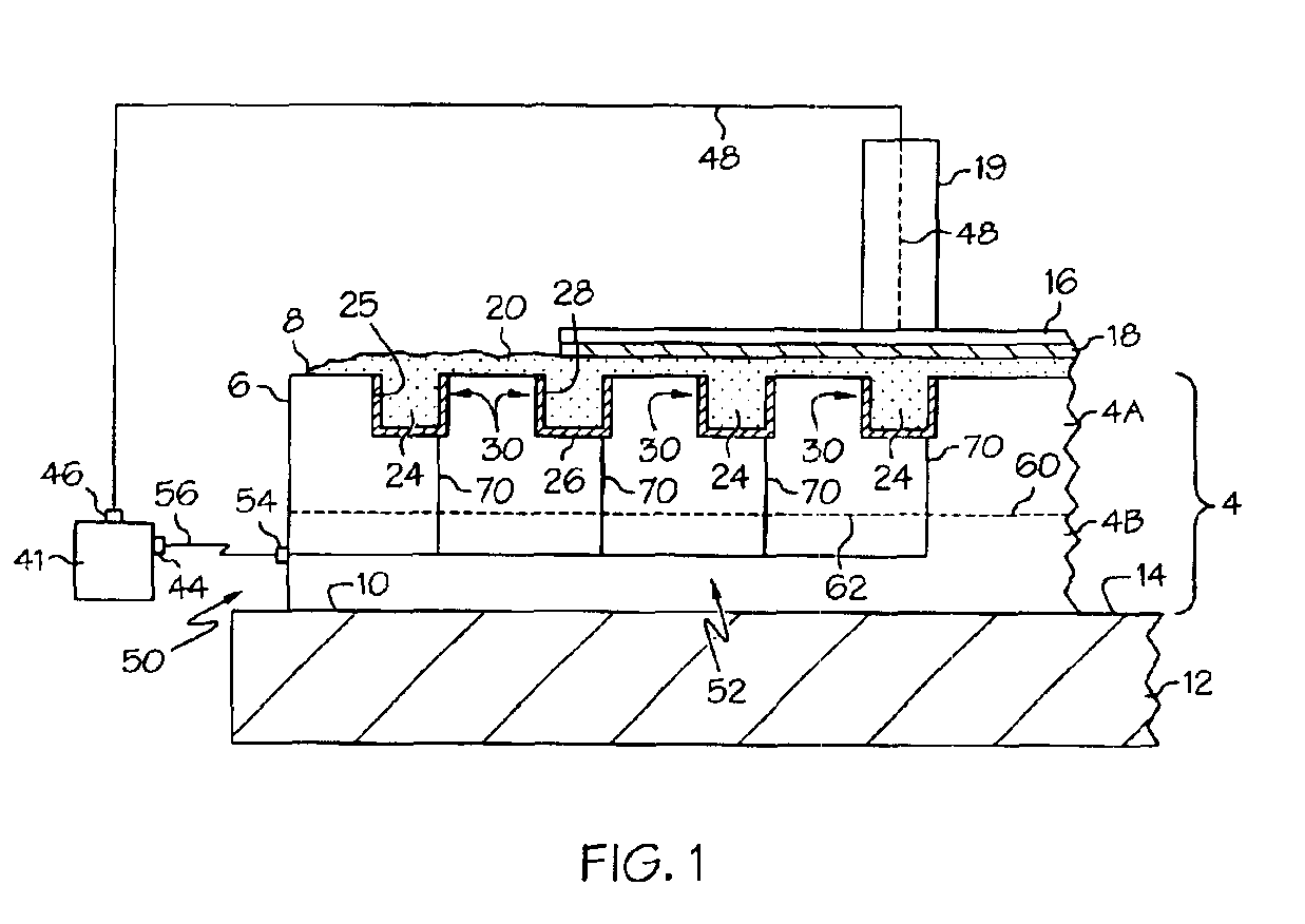
[0017]Referring to the drawings, FIG. 1 is a cross-sectional diagram of the polishing pad 4 of the present invention, shown as part of an ECMP system. Pad 4 has an upper surface 8 and a lower surface 10. Upper surface 8 serves as the polishing surface. Polishing pad 4 is supported by a platen 12 with an upper surface 14. A substrate (e.g., a wafer) 16 having a metal layer 18 is held in a substrate carrier 19 and positioned in contact with or in very close proximity to pad upper surface 8. An electrolytic polishing fluid 20 is disposed between polishing pad upper surface 8 and substrate metal layer 18.

[0018]Polishing...


PUM

PropertyMeasurementUnit
Thicknessaaaaaaaaaa
Lengthaaaaaaaaaa
Lengthaaaaaaaaaa

Abstract

The present invention provides a polishing pad for electrochemical mechanical polishing of conductive substrate. The pad comprises a plurality of grooves formed in a polishing surface of the polishing pad, the grooves being adapted to facilitate the flow of polishing fluid over the polishing pad. The conductive layers are respectively formed in the grooves and are in electrical communication with each other.

Description

BACKGROUND OF THE INVENTION[0002]The invention generally relates to polishing pads for chemical mechanical polishing (CMW), in particular, the invention relates to polishing pads for electrochemical mechanical polishing (ECMP), including methods and systems therefor.[0003]In the fabrication of integrated circuits and other electronic devices, multiple layers of conducting, semiconducting, and dielectric materials are deposited on or removed from the surface of a semiconductor wafer. Thin layers of conducting, semiconducting, and dielectric materials are deposited by a number of deposition techniques. Common deposition techniques include physical vapor deposition (PVD), also known as sputtering, chemical vapor deposition (CVD), plasma-enhanced chemical vapor deposition (PECVD), and electrochemical plating (ECP).[0004]As layers of materials are sequentially deposited and removed, the uppermost surface of the wafer becomes non-planar. Because subsequent semiconductor processing (e.g., ...

Claims


Application Information

Patent Timeline
IPC IPC(8): B24B1/00B24B37/00B24B37/04H01L21/02H01L21/304H01L21/302
CPCB24B37/26B24B37/042
Inventor COOK, LEE MELBOURNEJAMES, DAVID B.ROBERTS, JOHN V. H.
Owner ROHM & HAAS ELECTRONICS MATERIALS CMP HLDG INC
Why Eureka
Try Eureka