Growing a low defect gallium nitride based semiconductor

Inactive Publication Date: 2005-02-01
LUMILEDS
View PDF7 Cites 5 Cited by
  • Summary
  • Abstract
  • Description
  • Claims
  • Application Information

AI Technical Summary

Benefits of technology

It is a further object of the present invention to provide an edge emitting diode tha

Problems solved by technology

First, the structure has poor heat dissipation.
The path to the substrate is restricted by the width of the ridge structure; hence, removing heat by transferring the heat to the substrate, which is typically in thermal contact with a heat sink, is difficult.
The second problem with ridge structured devices is the high voltages needed to operate the devices.
However, the available area is limited by the area on the top of the ridge.

Method used


Image

  • Growing a low defect gallium nitride based semiconductor
  • Growing a low defect gallium nitride based semiconductor
  • Growing a low defect gallium nitride based semiconductor

Examples


Embodiment Construction

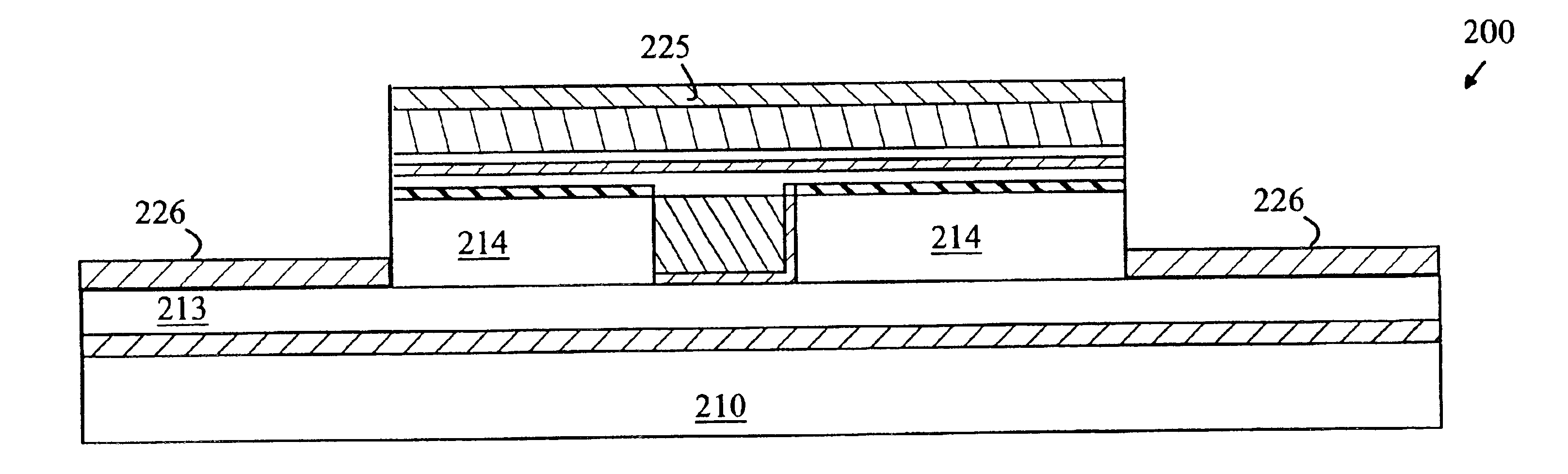
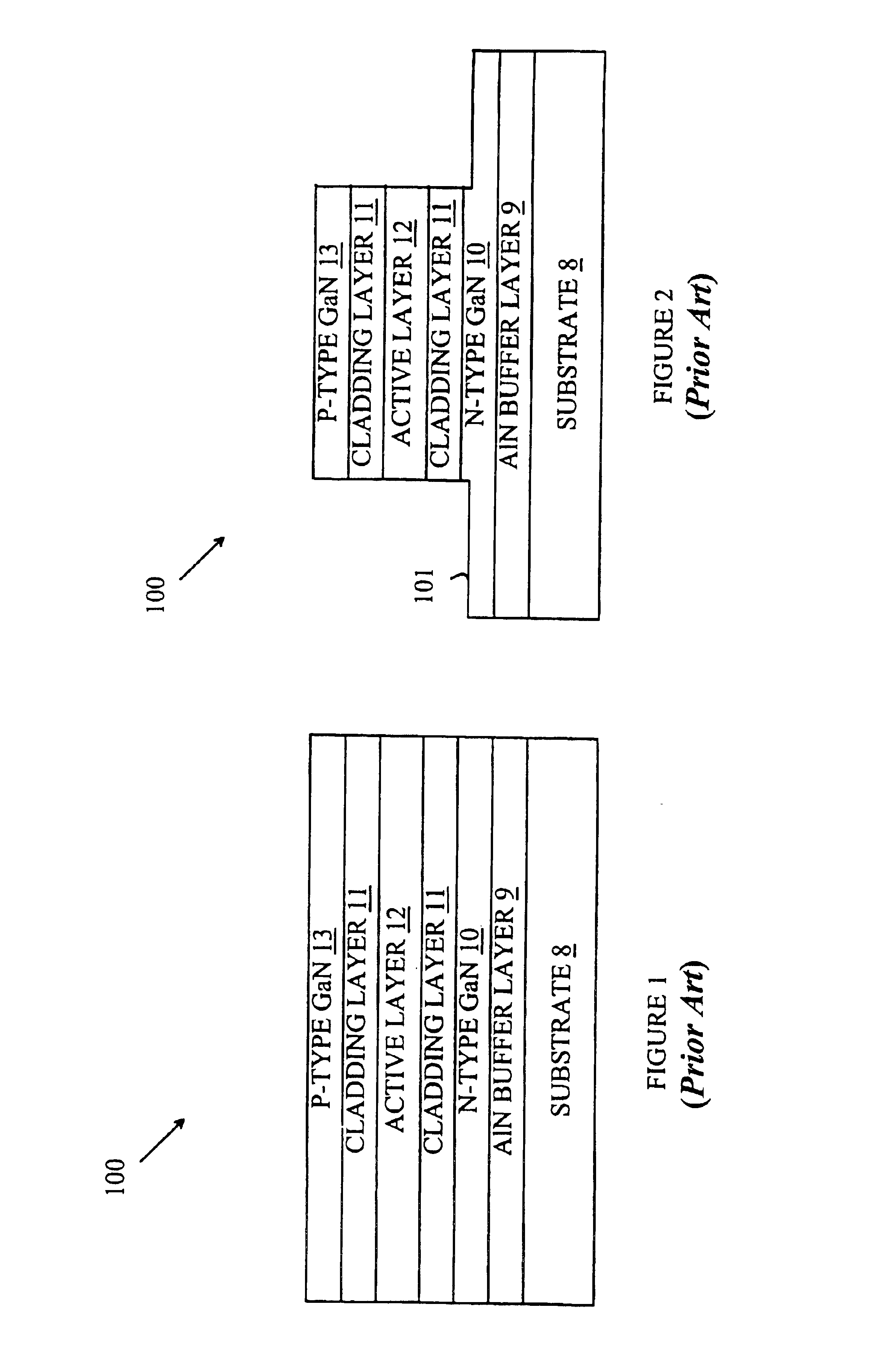
The present invention may be more easily understood with reference to FIGS. 1 and 2, which illustrate the fabrication of a typical prior art laser diode 100. Refer now to FIG. 1 which is a cross-sectional view of the layers deposited on a sapphire substrate 8 as the first step in fabricating a LD 100. An AIN layer is deposited by metal-organic chemical vapor deposition (MOCVD). AIN is preferred as the buffer material because a flat film consisting of a GaN single crystal is easily formed on an AlN layer.

After depositing the AlN buffer layer 9, a layer 10 of n-type GaN is deposited. The light-emitting part of the layer composed of GaN based cladding layers 11 and a GaN based active layer 12, and a p-type GaN layer 13 are deposited on layer 10. The cladding layers form the top and bottom walls of the laser waveguide. Referring to FIG. 2, the layers are then etched to create the side walls of the waveguide and to expose the n-type contact as shown at 101. The exposed area is used to ma...


PUM


Abstract

A low defect gallium nitride based semiconductor, and method for its production, is disclosed. A first gallium nitride based semiconductor layer overlying a substrate of a dissimilar material is grown. A trench is formed in the first gallium nitride based semiconductor layer. A material is deposited on a surface of the first gallium nitride based semiconductor layer to prevent a second gallium nitride based semiconductor layer, of a material different from the first gallium nitride based semiconductor layer, from nucleating thereon. The bottom surface of the trench is of a material such that the second gallium nitride based semiconductor layer will not nucleate thereon. The second gallium nitride based semiconductor material is grown, extending from at least one of the side walls of the trench, the second gallium nitride based semiconductor material having fewer defects than the first gallium nitride based semiconductor layer.

Description

FIELD OF THE INVENTIONThe present invention relates to semiconductor laser diodes and more particularly relates to edge-emitting semiconductor lasers.BACKGROUND OF THE INVENTIONBlue laser diodes (LDs) have the potential for increasing the storage capacity of optical disks over the densities currently available in compact disk systems based on red laser diodes. Increased storage capacity will open new markets for compact disks in motion picture distribution.One class of blue emitting elements is based on group III-V nitride films such as GaN epilayers grown on sapphire substrates. To fabricate a laser, a ridge structure is constructed to provide an appropriate optical cavity having parallel mirrors at each end of the cavity. The laser cavity is typically formed by sandwiching an active gain layer between two layers of GaN doped to form n-type and p-type semiconductors. The GaN layers are constructed so as to form a waveguide by depositing the various layers and then etching the stack...

Claims


Application Information

Patent Timeline
IPC IPC(8): H01S5/323H01S5/00H01S5/343H01S5/223H01S5/227H01S5/22
CPCB82Y20/00H01S5/32341H01S5/2232H01S5/227H01S2304/12H01S5/34333H01S2304/00H01S2304/04
Inventor WANG, SHIH-YUANCHEN, YONG
Owner LUMILEDS
Why Eureka
Try Eureka