

Process for separating dies on a wafer
- Summary
- Abstract
- Description
- Claims
- Application Information
AI Technical Summary
Benefits of technology
Problems solved by technology
Method used
Image

Examples
first embodiment
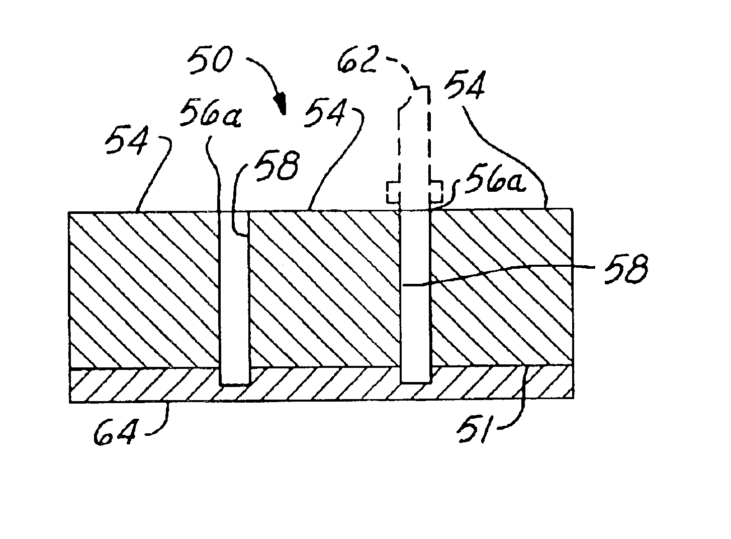
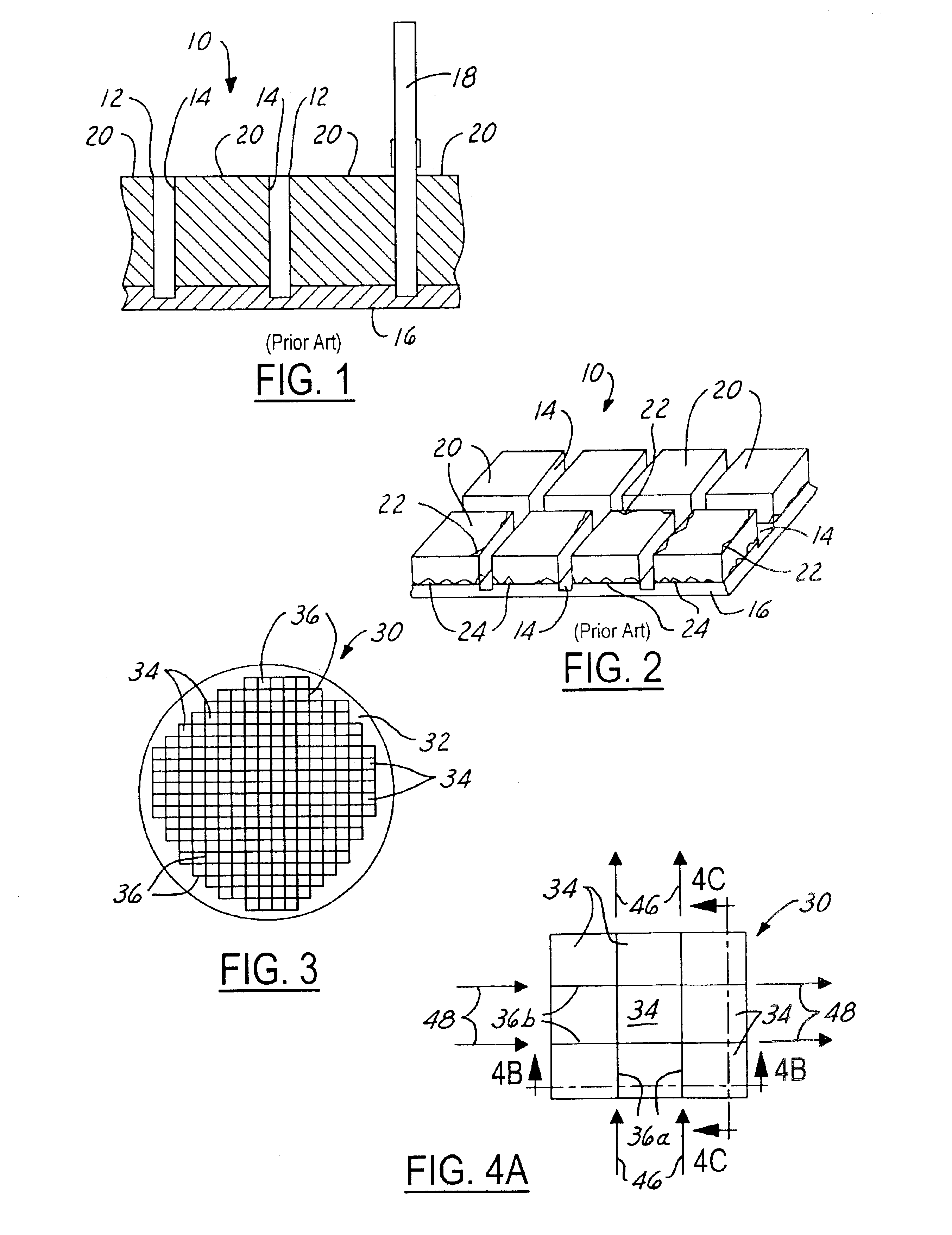
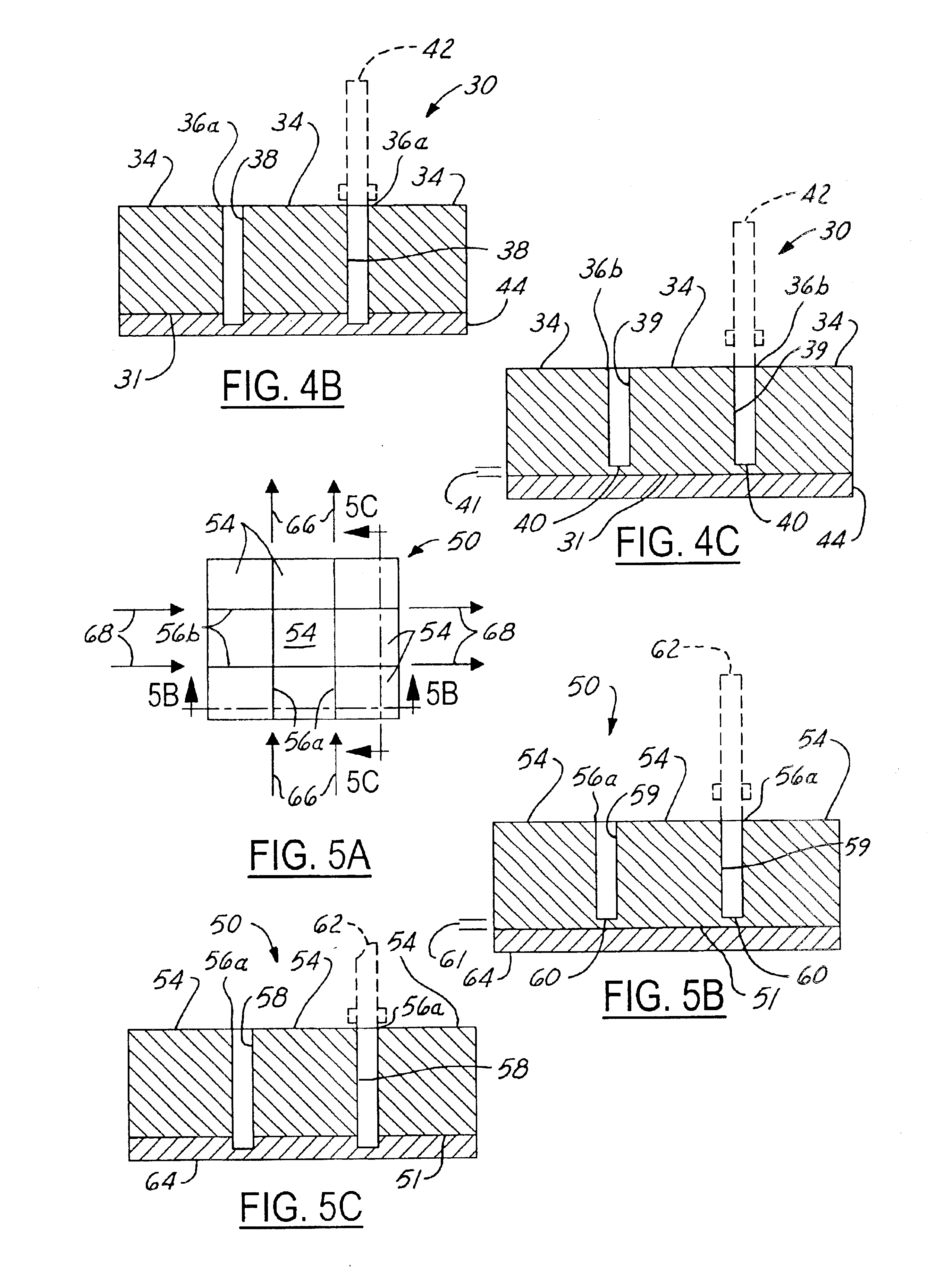
In the process of the present invention, the IC dies 34 are separated from each other in the wafer 30 as follows. In a first step of the process, a saw blade 42 of a wafer-cutting saw (not shown), which may be conventional, is used to cut complete separation channels 38 through the entire thickness or vertical dimension of the wafer 30, as shown in FIG. 4B, in the X-axis direction 46 and along the X-axis scribe lines 36a on the wafer 30, as shown in FIG. 4A. Accordingly, as further shown in FIG. 4B, the complete separation channels 38 completely separate adjacent dies 34 on the wafer 30 and may extend into the underlying adhesive tape 44. Typically, but not necessarily, the complete separation channels 38 extend about halfway through the thickness of the underlying adhesive tape 44, leaving at least the bottom half thickness of the adhesive tape 44 intact.
In a second step of the process, the saw blade 42 is used to cut partial separation channels 39 through most of the thickness or ...
PUM
 Abstract
Description
Claims
Application Information