
Semiconductor wafer protection and cleaning for device separation using laser ablation

a technology of laser ablation and semiconductors, applied in the field of semiconductor device separation, can solve the problems of reducing the reliability of the device, affecting the efficiency of the device, and accumulating waste materials on the wafer, so as to reduce the processing steps and reduce the processing. the effect of waste, reducing the amount of waste, and improving the process efficiency

Inactive Publication Date: 2005-02-01
POWER INTEGRATIONS INC +1
View PDF35 Cites 60 Cited by
  • Summary
  • Abstract
  • Description
  • Claims
  • Application Information

AI Technical Summary

Benefits of technology

A method according to the principles of the present invention provides for efficient device separation processing by using compatible materials. In one aspect, processing steps are minimized by choosing compatible materials for mounting the wafer, protecting the devices and cleaning off the protective coating. In one embodiment, the method includes the step of applying a protective coating on the side to be cut of a semiconductor wafer, mounting the other side of the semiconductor wafer on a mounting material such as an adhesive tape, cutting the semiconductor with a laser beam, and cleaning the wafer with a cleaning agent. The mounting material, the cleaning agent, and the protective coating are selected such that the cleaning agent does not damage the mounting material but removes the protective coating. Specifically, when an adhesive tape is used as the mounting material, the cleaning agent does not damage the adhesive and the tape forming the adhesive tape. As a result, the semiconductor wafer remains on the mounting material during and after the cleaning process, increasing the efficiency of the process.
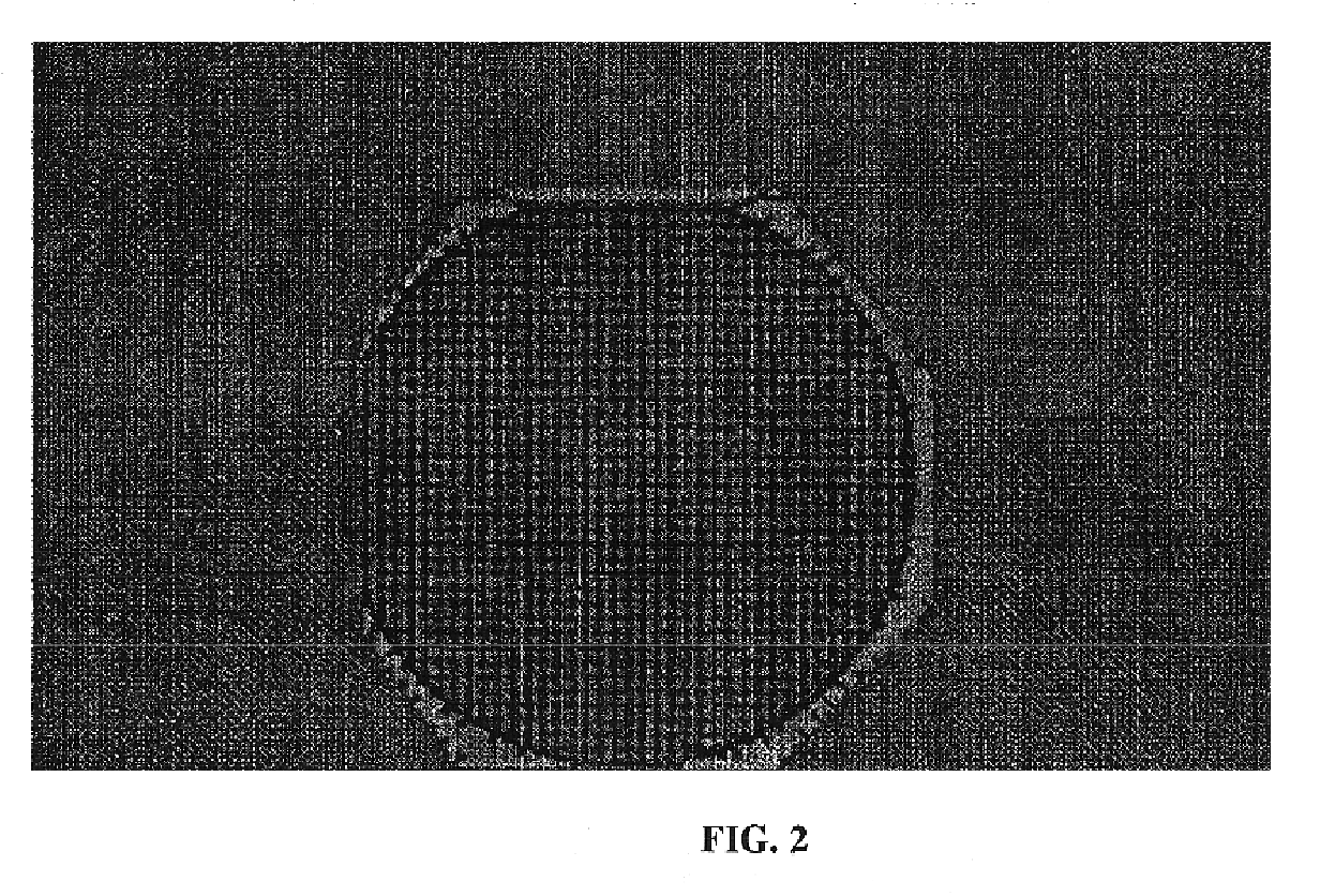
In another exemplary embodiment, the method of the invention includes the following steps: applying a protective coating on the side to be cut of a wafer with sapphire substrate, mounting the other side of the wafer on an adhesive tape, mounting the wafer with the adhesive tape on a cutting table, cutting the wafer with a laser, breaking the wafer into die, and cleaning the wafer by a wet etch with a cleaning solution. The cleaning solution, the protective coating, and the adhesive tape are selected such that the cleaning solution removes slag resulting from the cutting, debris resulting from the breaking, and the protective coating, but does not damage the adhesive tape, so that the die can remain on the adhesive tape before, during and after the cleaning.

Problems solved by technology

Because scribing removes material from the wafer, some scribing techniques can result in the buildup of waste material on the wafer.
That is, there tends to be more slag near the top of the cut than the bottom.
Slag around the die perimeter can degrade the reliability of the device and inhibit wire bonding.
In optical devices, such as LED's and lasers, sidewall buildup can decrease the power output of the device, as the slag can absorb some of the optical output power of the device.

Method used


Image

  • Semiconductor wafer protection and cleaning for device separation using laser ablation
  • Semiconductor wafer protection and cleaning for device separation using laser ablation
  • Semiconductor wafer protection and cleaning for device separation using laser ablation

Examples


Embodiment Construction

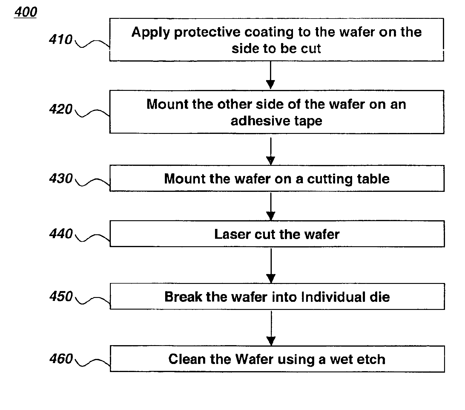
With reference to the figures for purposes of illustration, the present invention relates generally to an efficient process for die separation. Because of the large amount of energy needed to remove sapphire from a cut area using laser ablation, the waste sapphire tends to form a residue that cannot be removed easily. This waste, or slag, as it is commonly referred to, has two effects on subsequent die yield from the separation process. First, the top surface of the die has been found to have a large buildup of material around the perimeter of the die that degrades reliability and prevents wire bonding of the die. If the die size is generally less than 0.5 mm square, the entire surface can be covered by slag as illustrated by FIG. 1. Secondly, sidewalls of the die which are exposed during ablation have a slag buildup that increases from the bottom to the top of the cut. This excess material decreases the output power of the die since it is absorbing. Given that the comparable hardne...


PUM


Abstract

A method of protecting and cleaning a semiconductor wafer using laser ablation includes the following steps: applies a protective coating on the side to be cut of a wafer with sapphire substrate, mounts the other side of the sapphire wafer on an adhesive tape, mounts the sapphire wafer on a cutting table, cuts the sapphire wafer with a laser, breaks the sapphire wafer into die, and cleans the sapphire wafer with a cleaning solution that removes slag resulting from the cutting, debris resulting from the breaking, and the protective coating, but the adhesive tape, the cleaning solution, and the protective coating are selected such that the cleaning solution does not damage the adhesive tape.

Description

FIELD OF THE INVENTIONThis invention relates to the field of semiconductor fabrication, and more particularly to semiconductor device separation.BACKGROUND OF THE INVENTIONIn the field of semiconductor device fabrication, there are various methods for separating a wafer into die, including scribe and break techniques. In scribe and break techniques, the die is separated by breaking the wafer along scribe lines, which can be cut in the wafer in a number of ways. For example, wafers having semiconductor substrates can be mechanically scribed, such as with a diamond. In wafers having sapphire substrates, laser scribing has been disclosed, as, for example, in U.S. patent application No. 09 / 178,287, entitled, “Semiconductor Device Separation Using a Patterned Laser Projection,” which is incorporated herein by reference. The device separation method disclosed therein uses laser ablation to form scribe lines in the wafer.Because scribing removes material from the wafer, some scribing techn...

Claims


Application Information

Patent Timeline
Patent Type & Authority Patents(United States)
IPC IPC(8): H01L21/02H01L21/301H01L21/302H01L21/46H01L21/70H01L21/78B23K26/073B23K26/40H01L21/304H01L33/00
CPCB23K26/0656B23K26/0738B23K26/367B23K26/4075H01L21/6836H01L21/78H01L2924/0002B23K2201/40H01L21/3043H01L33/0095H01L2221/68327H01L2221/6834Y10S438/94H01L2924/00B23K2101/40B23K2103/50B23K26/364B23K26/066B23K26/40
Inventor SHELTON, BRYAN S.GOTTFRIED, MARKSCHWED, STEPHENELIASHEVICH, IVAN
Owner POWER INTEGRATIONS INC
Learn More