Method of producing biaxially textured buffer layers and related articles, devices and systems

Active Publication Date: 2005-02-01
FLORIDA UNIV OF A FLORIDA +1
View PDF6 Cites 40 Cited by
  • Summary
  • Abstract
  • Description
  • Claims
  • Application Information

AI Technical Summary

Benefits of technology

[0017]A power transformer includes a primary winding, and a secondary winding, wherein at least one of the primary winding and secondary winding compr

Problems solved by technology

While the above-described IBAD process has provided the desired biaxial texture requiring a relatively high thickness (>1 μm), such as by use of a YSZ film deposited in the presence of the Ar+ beam, the process is relatively slow and as a result expensive.
The speed and price of such process is a significant issue in the large-scal

Method used


Image

  • Method of producing biaxially textured buffer layers and related articles, devices and systems
  • Method of producing biaxially textured buffer layers and related articles, devices and systems
  • Method of producing biaxially textured buffer layers and related articles, devices and systems

Examples


example 1

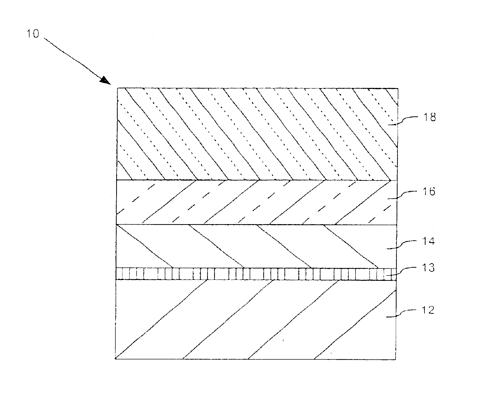
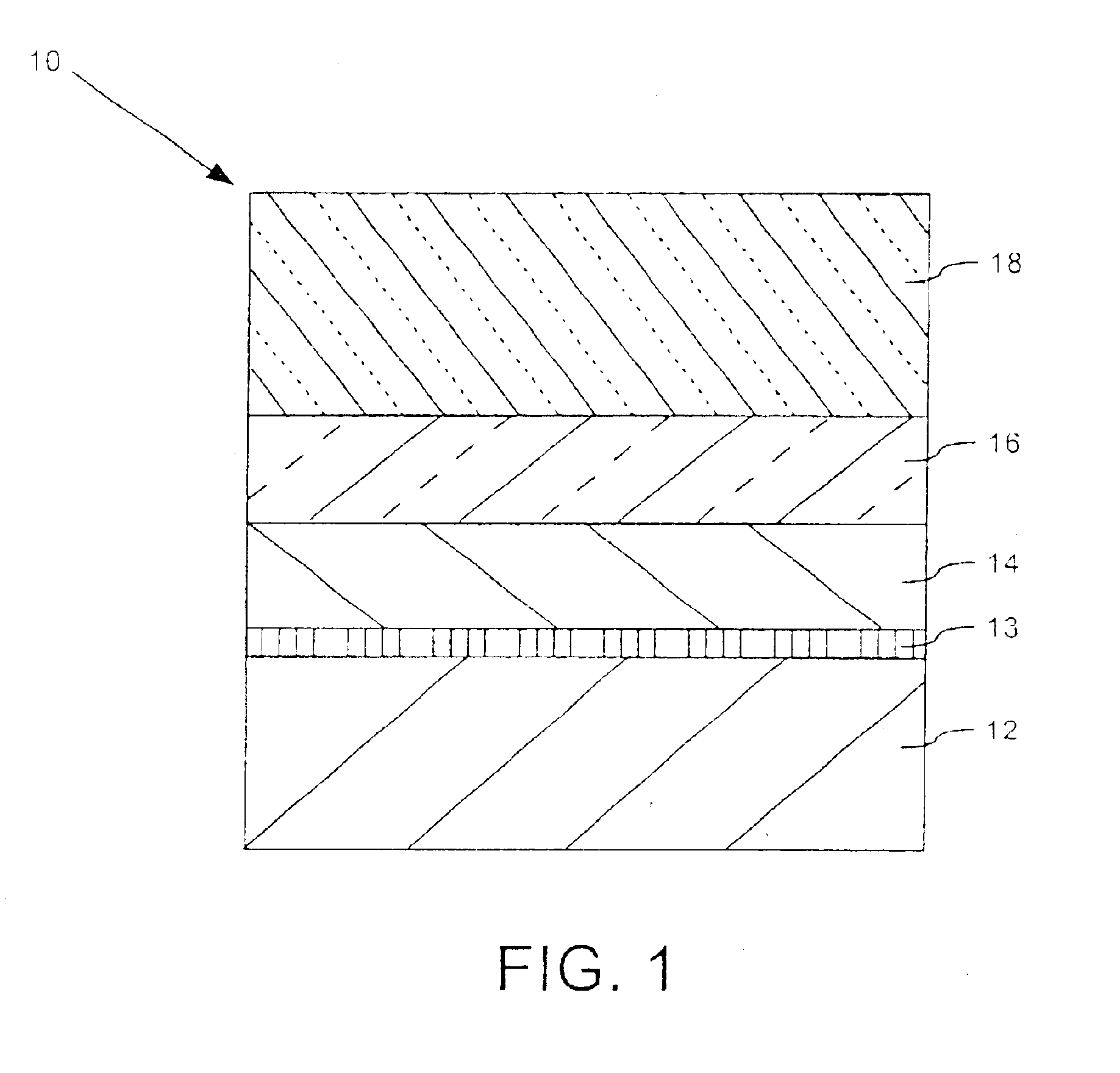
[0055]A Ni-based alloy substrate is provided for film growth. The substrate is cleaned with solvents, such as acetone, methanol, and trichloroethylene. The substrate is mounted in a pulsed-laser deposition chamber for thin film deposition. A polycrystalline yttria-stabilized zirconia (YSZ) protective layer is deposited on the substrate using pulsed laser deposition at about 25° C. under vacuum. This protective layer prevents chemical reactions between layer 1 and the substrate.

[0056]The coated substrate is heated to about 700° C. in vacuum for the deposition of an YBa2Cu3O7 thin film (Layer 1). A YBa2Cu3O7 film of thickness about 300 nm is deposited at about 700° C. in about 200 mTorr of oxygen. The film is c-axis oriented, but randomly oriented in-plane. The substrate is then transferred to a thin-film deposition system equipped with an ion gun. The substrate is heated to a temperature suitable for the epitaxial growth of MgO on YBa2Cu3O7 on Layer 1. Pulsed laser deposition is empl...

example 2

[0057]A Ni-based alloy substrate is provided for film growth. The substrate is cleaned with solvents, such as acetone, methanol, and trichloroethylene. The substrate is mounted in a pulsed-laser deposition chamber for thin film deposition. A MgO film of thickness of about 100 nm (Layer 1) is deposited at about 25° C. in vacuum. The MgO layer will be (001) textured. The coated substrate is then transferred to a thin-film deposition system equipped with an ion gun. A second layer of MgO (Layer 2) is grown in the presence of an Ar ion beam, the ion beam being directed along either the [111] or [110] crystallographic direction of MgO. The second MgO layer (Layer 2) will be biaxially textured.


PUM


Abstract

A superconductor article includes a substrate and a first buffer film disposed on the substrate. The first buffer film has a uniaxial crystal texture characterized (i) texture in a first crystallographic direction that extends out-of-plane of the first buffer film with no significant texture in a second direction that extends in-plane of the first buffer film, or (ii) texture in a first crystallographic direction that extends in-plane of the first buffer film with no significant texture in a second direction that extends out-of-plane of the first buffer film. A second buffer film is disposed on the first buffer film, the second buffer film having a biaxial crystal texture. A superconductor layer can be disposed on the second buffer film. Ion-beam assisted deposition (IBAD) can be used to deposit the second buffer film.

Description

CROSS-REFERENCE TO RELATED APPLICATIONS[0002]Not ApplicableSTATEMENT REGARDING FEDERALLY SPONSORED RESEARCH OR DEVELOPMENT[0003]Not applicableFIELD OF THE INVENTION[0004]The invention relates to biaxially textured buffer layers and articles, devices and systems made therefrom, including superconductor wires and tapes.BACKGROUND OF THE INVENTION[0005]Much of the effort to develop a high temperature superconducting (HTS) wire or tape has focused on coated conductors based on the epitaxial growth of high temperature superconducting (HTS) films on tapes that possess a biaxially-textured surface. Superconducting films with critical current densities in excess of 1 MA / cm2 at 77 K and self-field have been achieved for epitaxial YBa2Cu3O7 films on biaxially-textured tapes produced either by ion-beam assisted deposition (IBAD) or thermomechanically-textured metals.[0006]In previous work involving IBAD, the synthesis of the biaxially-textured buffer layer suitable for HTS films capable of car...

Claims


Application Information

Patent Timeline
IPC IPC(8): H01L39/24C30B25/18C30B29/22
CPCC30B25/18H01L39/2461C30B29/22Y10S428/93H10N60/0632H01B12/02
Inventor NORTON, DAVID P.SELVAMANICKAM, VENKAT
Owner FLORIDA UNIV OF A FLORIDA
Why Eureka
Try Eureka