Miniaturized dielectrically isolated solid state device

a dielectric isolation and solid state technology, applied in the direction of radioactive control devices, crystal growth processes, chemistry apparatus and processes, etc., can solve the problems of device failure mechanisms, surface failure, and still not perfect passivation, etc., and achieve the effect of novel effects

Inactive Publication Date: 2005-02-01
LI SECOND FAMILY
View PDF33 Cites 1 Cited by
  • Summary
  • Abstract
  • Description
  • Claims
  • Application Information

AI Technical Summary

Benefits of technology

[0011]Yet another object is to provide a semiconductor device with an enclosing isolation oxide region having a unique geometry, size, and position relative to the PN junction so as to achieve novel effects.
[0012]A further object is to form high-density, high-yield, but low-cost silicon integrated circuits with dielectrically isolated circuit components.
[0014]Still another object is to provide methods for low-cost, high-volume production of these new semiconductor devices. Various other objects and advantages, and a more complete understanding of the invention, will become apparent to those skilled in the art from the following description and claims, taken in conjunction with the accompanying drawing.

Problems solved by technology

These devices therefore often fall by surface failure mechanisms.
However, such a surface, being bare, is still not perfectly passivated.

Method used


Image

  • Miniaturized dielectrically isolated solid state device
  • Miniaturized dielectrically isolated solid state device
  • Miniaturized dielectrically isolated solid state device

Examples


Embodiment Construction

RAWING

[0015]For the purpose of illustrating the invention, there is shown in the drawing the forms which are particularly preferred. It is understood, however, that this invention is not necessarily limited to the precise arrangements and instrumentalities here shown but, instead, may combine the same described embodiments or their equivalents in various forms.

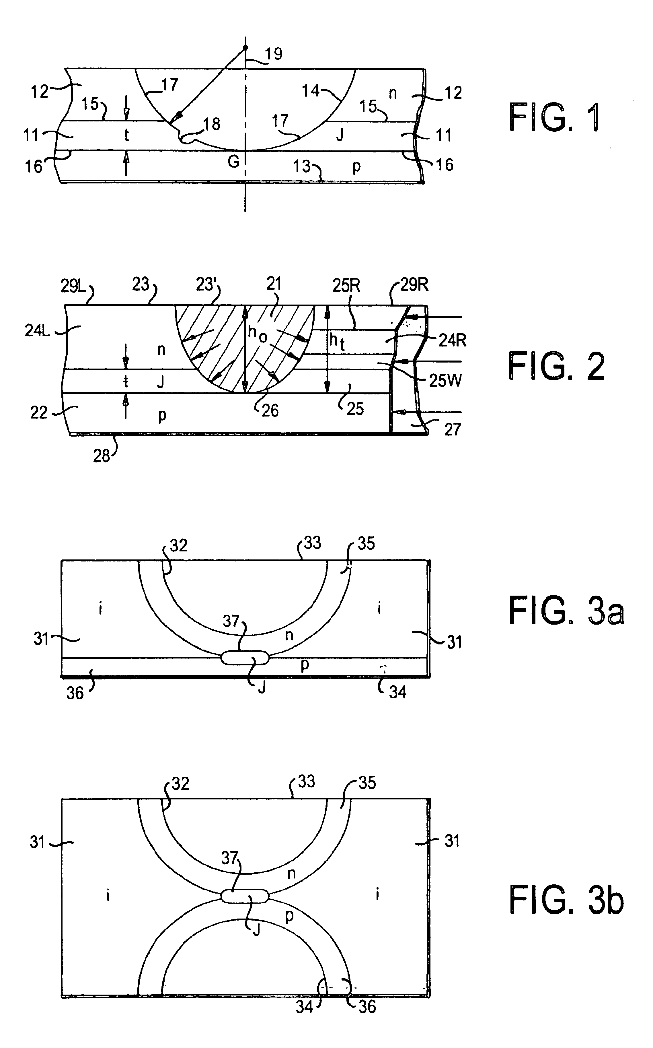
[0016]FIG. 1 is a partial cross-section of a semiconductor device having therein a curved-around, junction region peripheral surface and a gas-filled isolation groove;

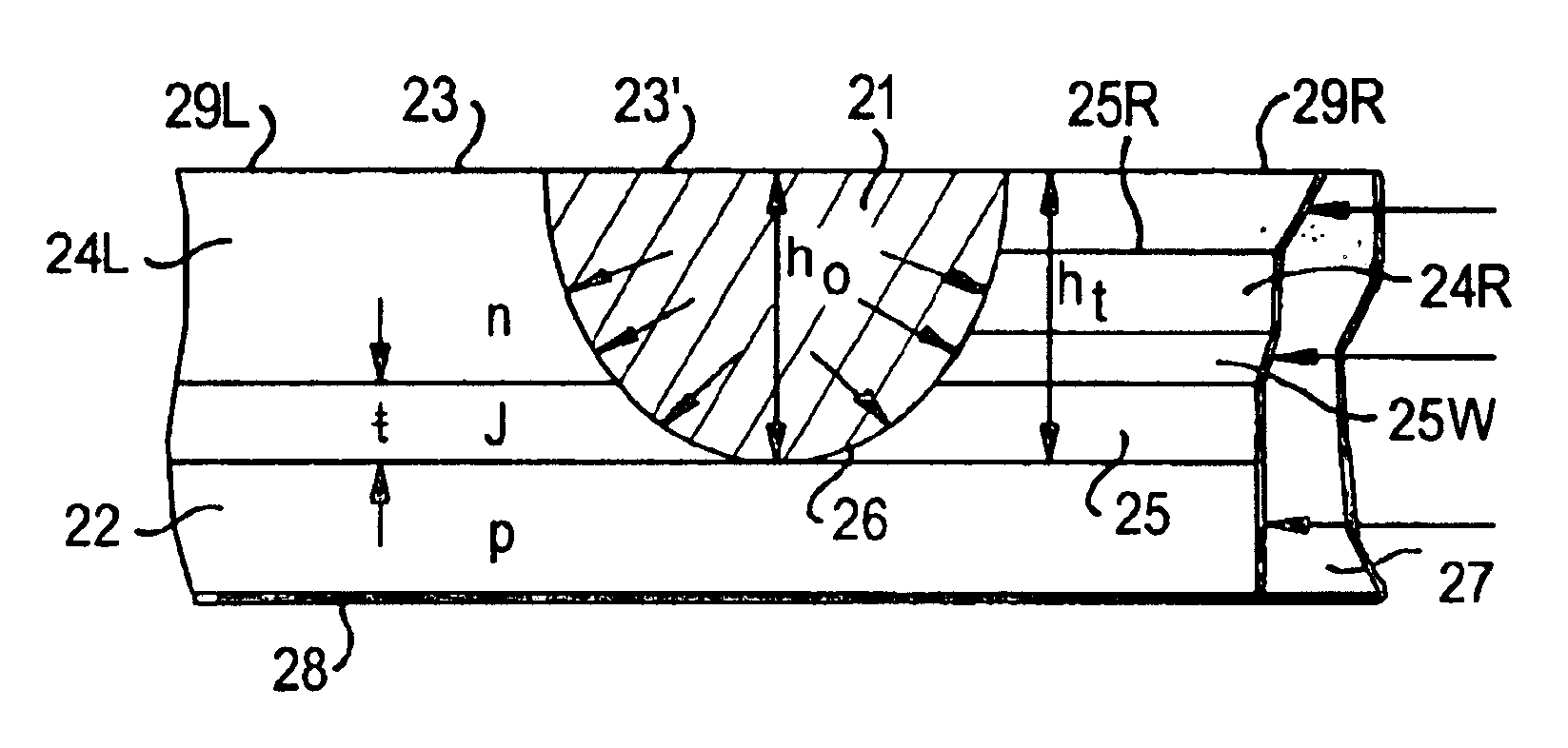
[0017]FIG. 2 shows portion of a silicon structure having a partly buried, PN junction region peripheral surface in contact with a round-bottomed, discretely in-situ formed silicon dioxide (or nitride) material region.

[0018]FIGS. 3a and 3b shows semiconductor devices having their PN junction region peripheral surfaces completely buried in intrinsic, or electronically inert, semiconductor materials;

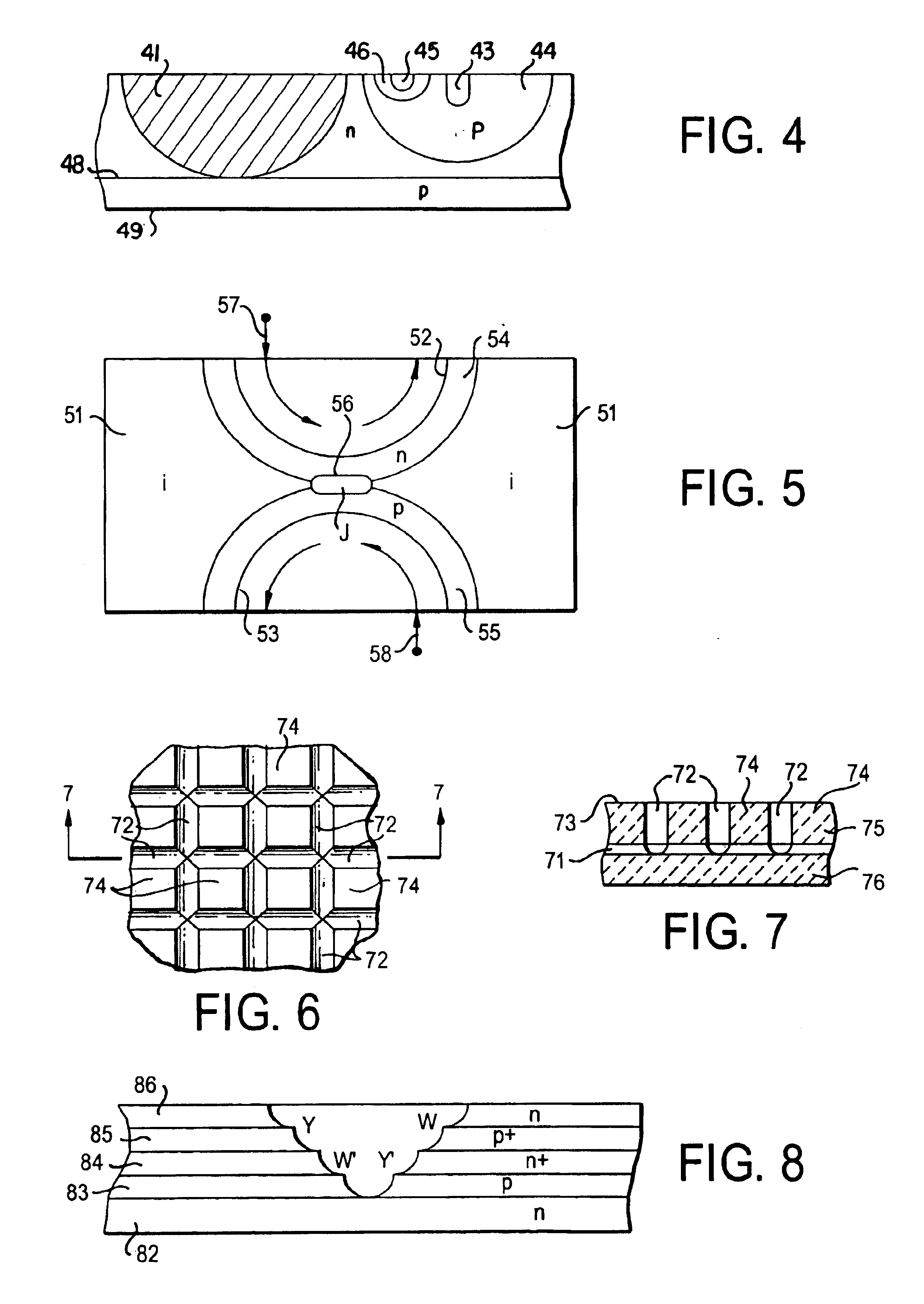
[0019]FIG. 4 shows npn transistor structure in a microcircuit made ...


PUM

PropertyMeasurementUnit
widthaaaaaaaaaa
temperatureaaaaaaaaaa

Abstract

An improved, surface-passivated and electrically isolated solid-state device (including integrated circuits) comprises a silicon wafer with a PN junction or other electronic rectifying barrier contained therein and thermally grown or ion-implanted oxide or nitride isolating grooves in-situ formed in the wafer to isolate it into a plurality of physically integral pockets for use as electrically separately operable components. The grooves have symmetrical, centrally rounded bottoms which are located within a few microns below the PN junction or rectifying barrier. Through the unique oxide / nitride forming conditions and through curvature, symmetry, and proximity effects, novel passivation and isolation results obtain.

Description

[0002]This is a continuation of parent application Ser. No. 07 / 809,460 filed Dec. 9, 1991 (abandoned), which in turn is a continuation-in-part (CIP) of application Ser. No. 07 / 438,692 filed Nov. 17, 1989 (U.S. Pat. No. 5,082,793), which in turn is a CIP of application Ser. No. 05 / 838,758 filed Oct. 3, 1977 (U.S. Pat. No. 4,916,513) and a continuation of application Ser. No. 05 / 386,102 filed Aug. 6, 1973 (U.S. Pat. No. 4,946,800), each of the latter two being a CIP of application Ser. No. 05 / 154,300 filed Jun. 18, 1971 (abandoned), which in turn is a CIP of application Ser. No. 04 / 761,646 filed Sep. 23, 1968 (U.S. Pat. No. 3,585,714), which in turn is a CIP of application Ser. No. 04 / 490,955 filed Sep. 28, 1965 (U.S. Pat. No. 3,430,109). I hereby incorporate each of the above patents and patent applications by reference into this application. Also related are application Ser. No. 08 / 446,423 filed May 22, 1995 (U.S. Pat. No. 5,696,402), and copending applications Ser. Nos. 08 / 483,937 ...

Claims


Application Information

Patent Timeline
Patent Type & Authority Patents(United States)
IPC IPC(8): C30B21/02C30B21/00C30B21/04H01L21/762H01L21/02H01L21/76H01L21/24H01L29/04H01L29/02H01L27/142H01L27/15H01L31/18H01L21/763H01L21/764H01L21/70H01L27/144H01L31/036H01L31/068H01L27/00H01L29/06H01L31/06H01L31/078H01L31/00H01L33/00H01L33/18H01L33/24
CPCC30B21/02H01L21/24H01L21/76H01L21/76232H01L21/763H01L21/764H01L27/00H01L27/142H01L27/1446H01L27/156H01L29/04H01L29/0657H01L29/0661H01L31/00H01L31/036H01L31/0687H01L31/078H01L31/18C30B21/04Y02E10/544H01L33/18H01L33/24
Inventor LI, CHOU H.
Owner LI SECOND FAMILY
Why Eureka
Try Eureka