Method and apparatus for calibrating a metrology tool

a metrology tool and calibrator technology, applied in semiconductor/solid-state device testing/measurement, optical radiation measurement, spectrophotometry/monochromators, etc., can solve the problem of limiting the requirement for tool-to-tool matching to less than five nanometers, affecting the accuracy and reducing the random errors of a metrology tool. the effect of reducing the disadvantages and problems of calibrating a metrology tool

Inactive Publication Date: 2005-02-01
TOPPAN PHOTOMASKS INC
View PDF11 Cites 13 Cited by
  • Summary
  • Abstract
  • Description
  • Claims
  • Application Information

AI Technical Summary

Benefits of technology

In accordance with the teachings of the present invention, disadvantages and problems associated with calibrating a metrology tool have been substantially reduced or eliminated. In a particular embodiment, a method for calibrating a metrology tool includes providing an artifact having a contrast enhanced feature that reduces random errors in a metrology tool during a measuring process.
In accordance with one embodiment of the present invention, a method for calibrating a metrology tool includes measuring a parameter of a contrast enhanced feature on an artifact in a metrology tool, where the contrast enhanced feature may reduce random errors in the metrology tool during the measuring process. The method further compares the measured parameter with an initial parameter associated with the artifact and adjusts the metrology tool until the measured parameter matches the initial parameter. Furthermore, an artifact formed in accordance with the teachings of the present invention may be used to calibrate a metrology tool used to measure features on a photomask or a semiconductor wafer.
In accordance with another embodiment of the present invention, an apparatus for calibrating a metrology tool includes a feature formed on at least a portion of the substrate. The feature includes an optical contrast that may reduce random errors in a metrology tool during a measuring process.
In accordance with a further embodiment of the present invention, a photomask includes a patterned layer formed on at least a portion of a substrate. A photomask parameter for a feature in the patterned layer may be measured by calibrating a metrology tool with an artifact that includes a contrast enhanced feature, which may reduce random errors in the metrology tool during a measuring process. The photomask parameter for the feature may then be measured by using the calibrated metrology tool.
Important technical advantages of certain embodiments of the present invention include an artifact that improves the precision and accuracy of the data collected by a metrology tool. One cause for random errors in a metrology tool when reading a mask location may be the limited optical contrast of a feature to its background. The artifact of the present invention may include features that have an enhanced optical contrast compared to the background. By increasing the optical contrast of the features, the metrology tool may be able to more precisely and accurately detect the edges of the features and therefore, obtain a more consistent measurement.
Another important technical advantage of certain embodiments of the present invention includes an artifact that improves the ability to detect and correct systematic errors in a metrology tool. As a metrology tool ages, malfunctions or drift in the optical imaging equipment used to measure the features may require adjustments to restore the metrology tool to proper working order. These malfunctions may be unidentifiable if there are too many random errors during operation. The artifact of the present invention reduces the number of random errors by using enhanced contrast features that may improve the inherent signal to noise factors. By reducing the random errors, systematic errors that occur in the metrology tool may be more easily detected and corrected.

Problems solved by technology

As semiconductor device dimensions in an integrated circuit (IC) become smaller, a specification associated with how the IC should be fabricated becomes more restrictive with respect to the amount of error that is allowable in the process.
Today, it is common for advanced photomasks to have specifications of less than forty nanometers, which may limit the requirements for tool-to-tool matching to less than five nanometers.
The accuracy of a metrology tool, however, may be affected by systematic and / or random error factors.
Tool matching, grid transfers and statistical process control methods may also be effected by random errors that limit the ability to accurately and directly apply measured data from the metrology tool to a higher level of certainty.

Method used


Image

  • Method and apparatus for calibrating a metrology tool
  • Method and apparatus for calibrating a metrology tool
  • Method and apparatus for calibrating a metrology tool

Examples


Embodiment Construction

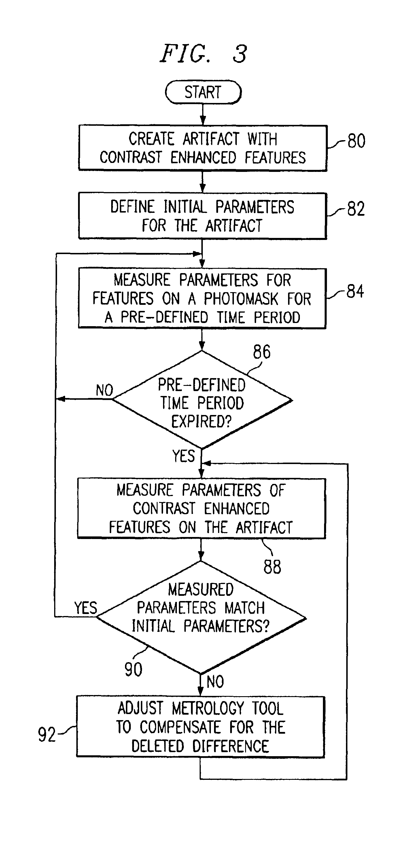
Preferred embodiments of the present invention and their advantages are best understood by references to FIGS. 1 through 3, where like numbers are used to indicate like and corresponding parts.

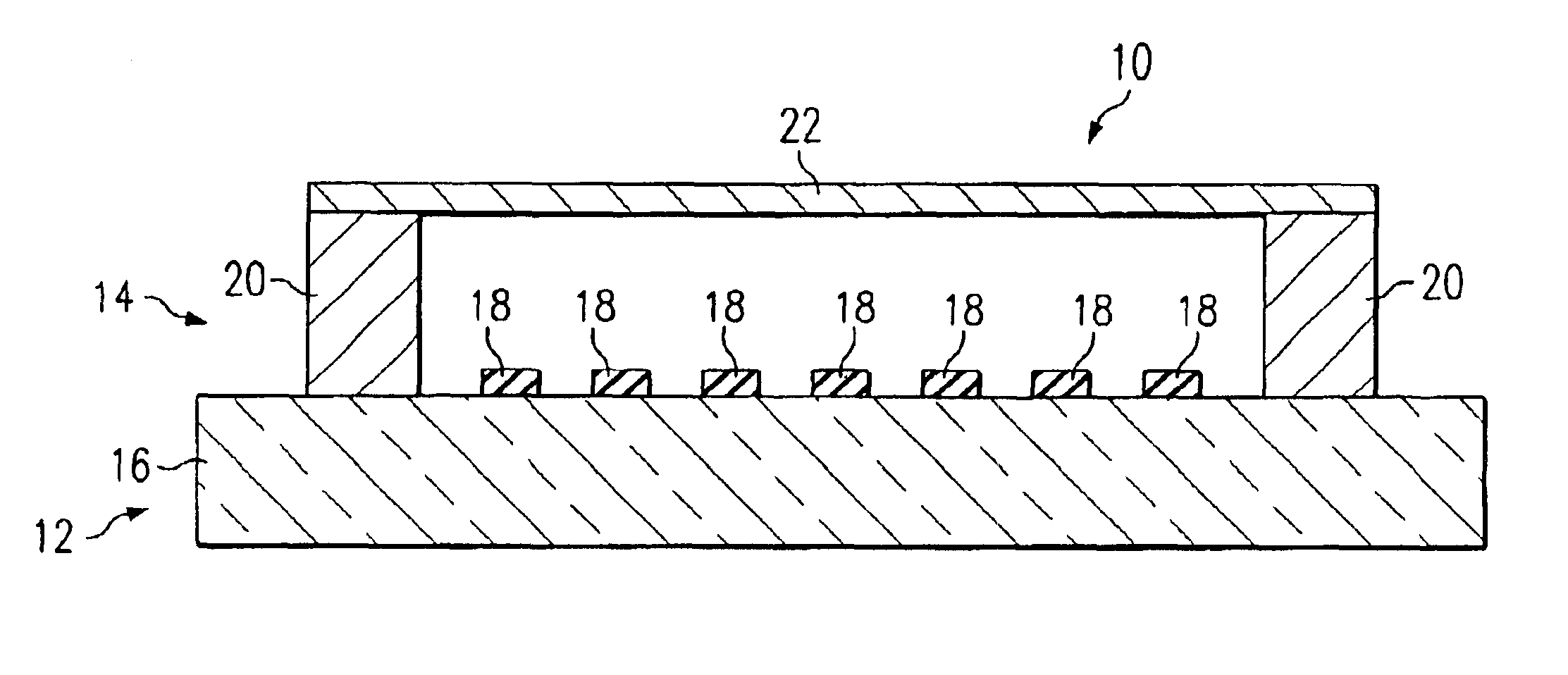
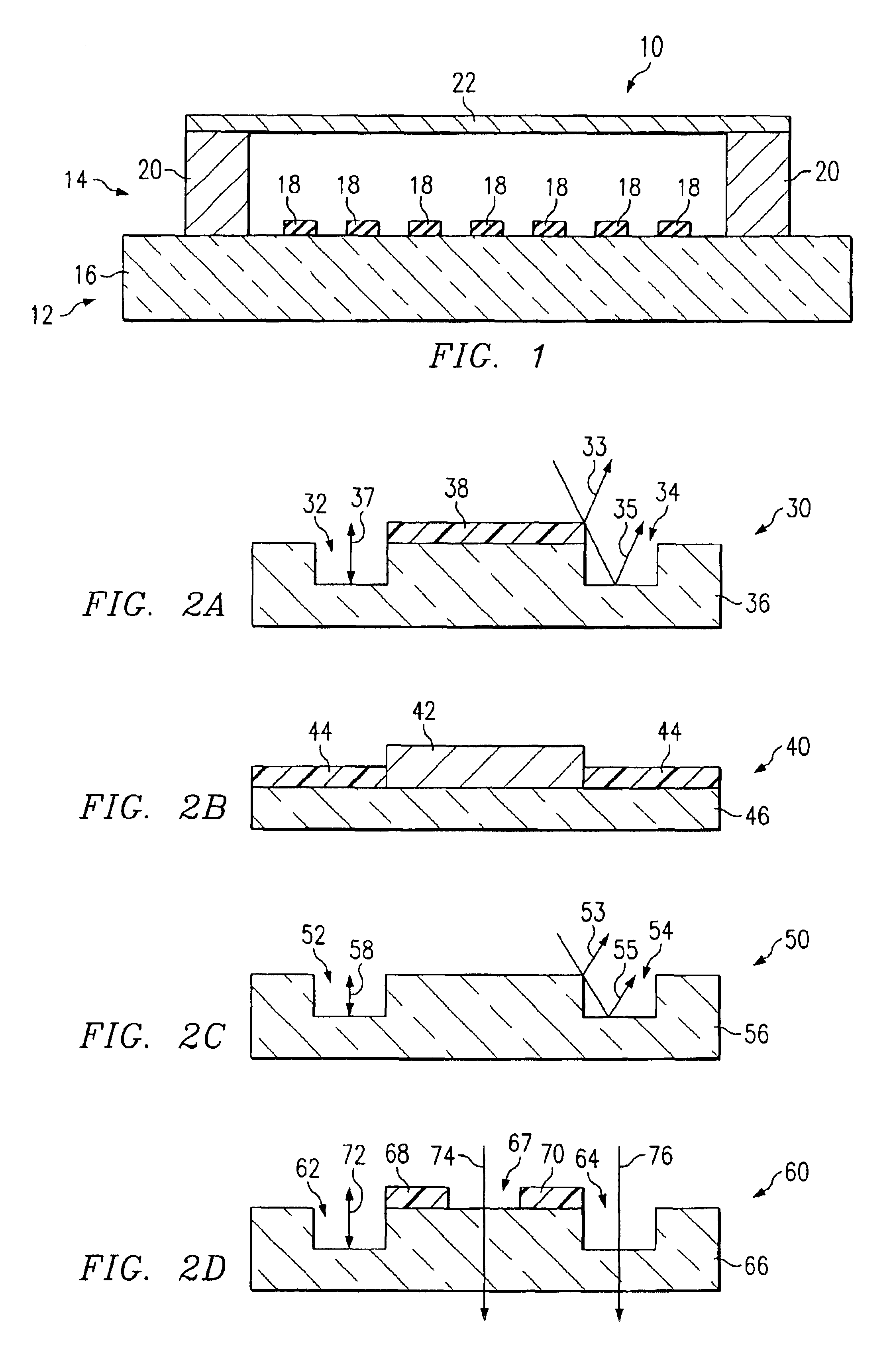
FIG. 1 illustrates a cross-sectional view of photomask assembly 10 qualified in a metrology tool calibrated with an artifact including contrast enhanced features. Photomask assembly 10 includes photomask 12 coupled to pellicle assembly 14. Substrate 16 and patterned layer 18 form photomask 12, otherwise known as a mask or reticle, that may have a variety of sizes and shapes, including but not limited to round, rectangular, or square. Photomask 12 may also be any variety of photomask types, including, but not limited to, a onetime master, a five-inch reticle, a six-inch reticle, a nine-inch reticle or any other appropriately sized reticle that may be used to project an image of a circuit pattern onto a semiconductor wafer. Photomask 12 may further be a binary mask, a phase shift mask (PSM), an ...


PUM

PropertyMeasurementUnit
transparentaaaaaaaaaa
wavelengthaaaaaaaaaa

Abstract

A method and apparatus for calibrating a metrology tool are disclosed. The method includes measuring a parameter of a contrast enhanced feature on an artifact using a metrology tool, where the contrast enhanced feature reduces random errors in the metrology tool during the measuring process. The measured parameter is compared with an initial parameter associated with the artifact and the metrology tool is adjusted until the measured parameter matches the initial parameter.

Description

TECHNICAL FIELD OF THE INVENTIONThis invention relates in general to the field of semiconductor device manufacturing and, more particularly, to a method and apparatus for calibrating a metrology tool.BACKGROUND OF THE INVENTIONAs semiconductor device dimensions in an integrated circuit (IC) become smaller, a specification associated with how the IC should be fabricated becomes more restrictive with respect to the amount of error that is allowable in the process. The specification may provide the requirements that a photomask, also known as a mask or reticle, must meet in order to be used to fabricate semiconductor devices on a wafer. For example, a specification may include the requirements for pattern position accuracy, feature size control and defect density for a specific manufacturing process.The pattern position accuracy and feature size control on an individual photomask may be measured by a metrology tool. Typically, a metrology tool should have no more than ten percent error...

Claims


Application Information

Patent Timeline
Patent Type & Authority Patents(United States)
IPC IPC(8): G01F25/00G01C19/00G01C25/00G01D18/00G06F19/00G03F1/00H01L23/544
CPCG03F1/84H01L22/34
Inventor WEST, CRAIG A.HUGHES, GREGORY P.IBSEN, KENT B.
Owner TOPPAN PHOTOMASKS INC
Why Eureka
Try Eureka