

Method and apparatus for decomposing semiconductor device patterns into phase and chrome regions for chromeless phase lithography
- Summary
- Abstract
- Description
- Claims
- Application Information
AI Technical Summary
Benefits of technology
Problems solved by technology
Method used
Image

Examples
Embodiment Construction
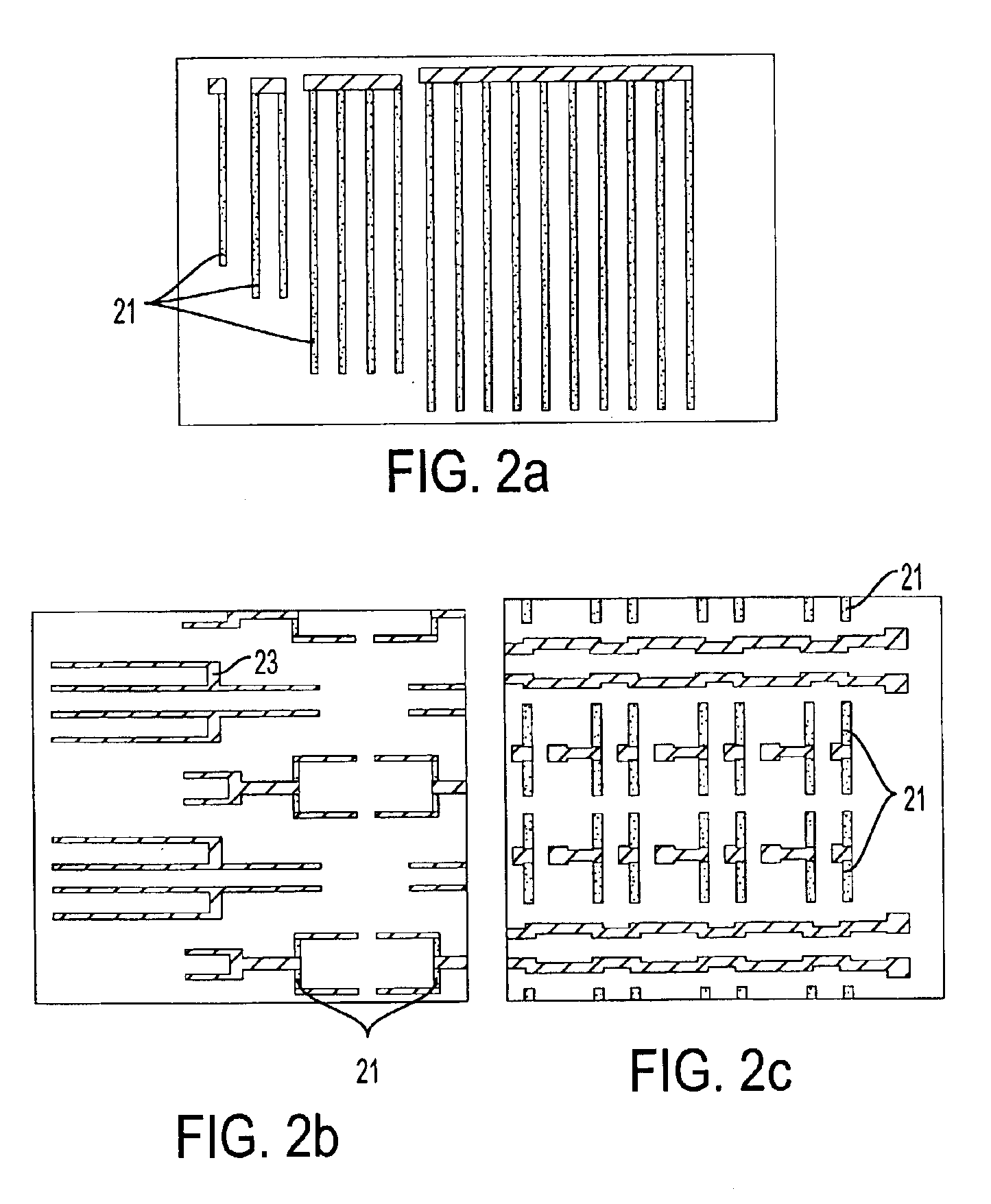
-5c represent the corresponding final mask design for the corresponding patterns set forth in FIGS. 2a, 3a and 4a; 2b, 3b and 4b; and 2c, 3c and 4c, respectively,
[0027]FIGS. 6a-6c illustrate various sub-resolution patterns capable of reducing flare.
[0028]FIG. 7 illustrates the relationship between the percentage transmission of a chrome sub-resolution pattern and the same pattern consisting of 180° phase-structures.
[0029]FIG. 8 schematically depicts a lithographic projection apparatus suitable for use with the masks designed with the aid of the current invention.
DETAILED DESCRIPTION OF THE INVENTION
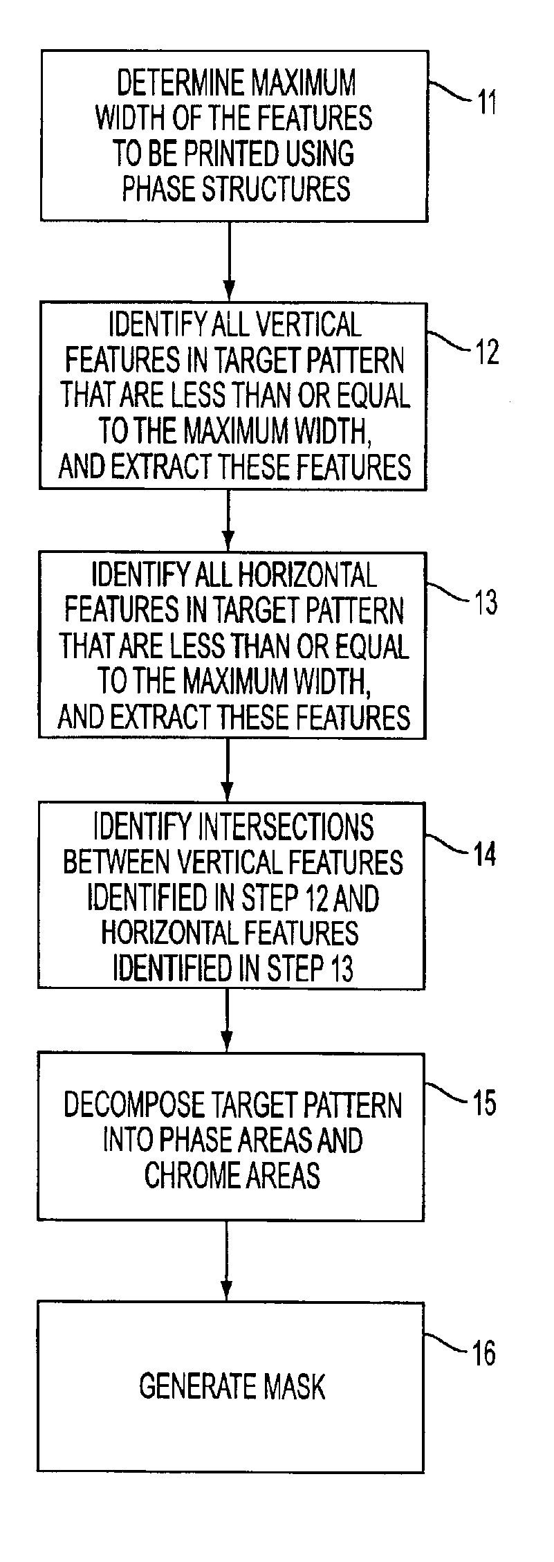
[0030]As explained in more detail below, the preferred embodiment of the present invention relates to a process for decomposing a desired target pattern (to be printed on a wafer) so as to produce a mask pattern (i.e., reticle) that can be utilized to image the wafer / substrate and generate the target pattern thereon. In accordance with the present invention, the mask pattern to be generat...
PUM
 Abstract
Description
Claims
Application Information