Substrate holding apparatus

a technology of holding apparatus and substrate, which is applied in the direction of grinding drive, manufacturing tools, lapping machines, etc., can solve the problems of increasing the step height on the surface of the semiconductor device, increasing the structure of the semiconductor element, and increasing the height of the semiconductor device. achieve the effect of uniform film thickness

Inactive Publication Date: 2005-02-08
EBARA CORP
View PDF12 Cites 49 Cited by
  • Summary
  • Abstract
  • Description
  • Claims
  • Application Information

AI Technical Summary

Benefits of technology

The present invention has been made in view of the above drawbacks. It is therefore an object of the present invention to provide a substrate holding apparatus capable of polishing a substrate such as a semiconductor wafer in accordance with a thickness distribution of thin film formed on a surface of the substrate, and obtaining uniformity of film thickness after polishing.

Problems solved by technology

Recently, semiconductor devices have become more integrated, and structure of semiconductor elements has become more complicated.
Therefore, irregularities on a surface of the semiconductor device are increased, so that a step height on the surface of the semiconductor device becomes larger.
When irregularities of a surface of a semiconductor device are increased, the following problems arise.
An open circuit is caused by disconnection of interconnections, or a short circuit is caused by insufficient insulation between layers.
As a result, good products cannot be obtained, and a yield is reduced.
Further, even if a semiconductor device initially works normally, reliability of the semiconductor device is lowered after a long-term use.
Therefore, if the irregularities of the surface of the semiconductor device are increased, then it is difficult to form a fine pattern on the semiconductor device.
If a pressing force produced between the semiconductor wafer and the polishing surface of the polishing pad is not uniform over an entire surface of the semiconductor wafer, then the semiconductor wafer is insufficiently or excessively polished depending on the pressing force applied to the semiconductor wafer.
The polishing pad is so elastic that the pressing force applied to a peripheral portion of the semiconductor wafer becomes non-uniform and hence the peripheral portion of the semiconductor wafer is excessively polished to cause edge rounding.
Therefore, a conventional substrate holding apparatus cannot realize a polishing amount distribution that is equal to the film thickness distribution on the surface of the semiconductor wafer, and hence cannot sufficiently cope with the film thickness distribution in the radial direction so as to cause insufficient or excessive polishing.

Method used


Image

  • Substrate holding apparatus
  • Substrate holding apparatus
  • Substrate holding apparatus

Examples


first embodiment

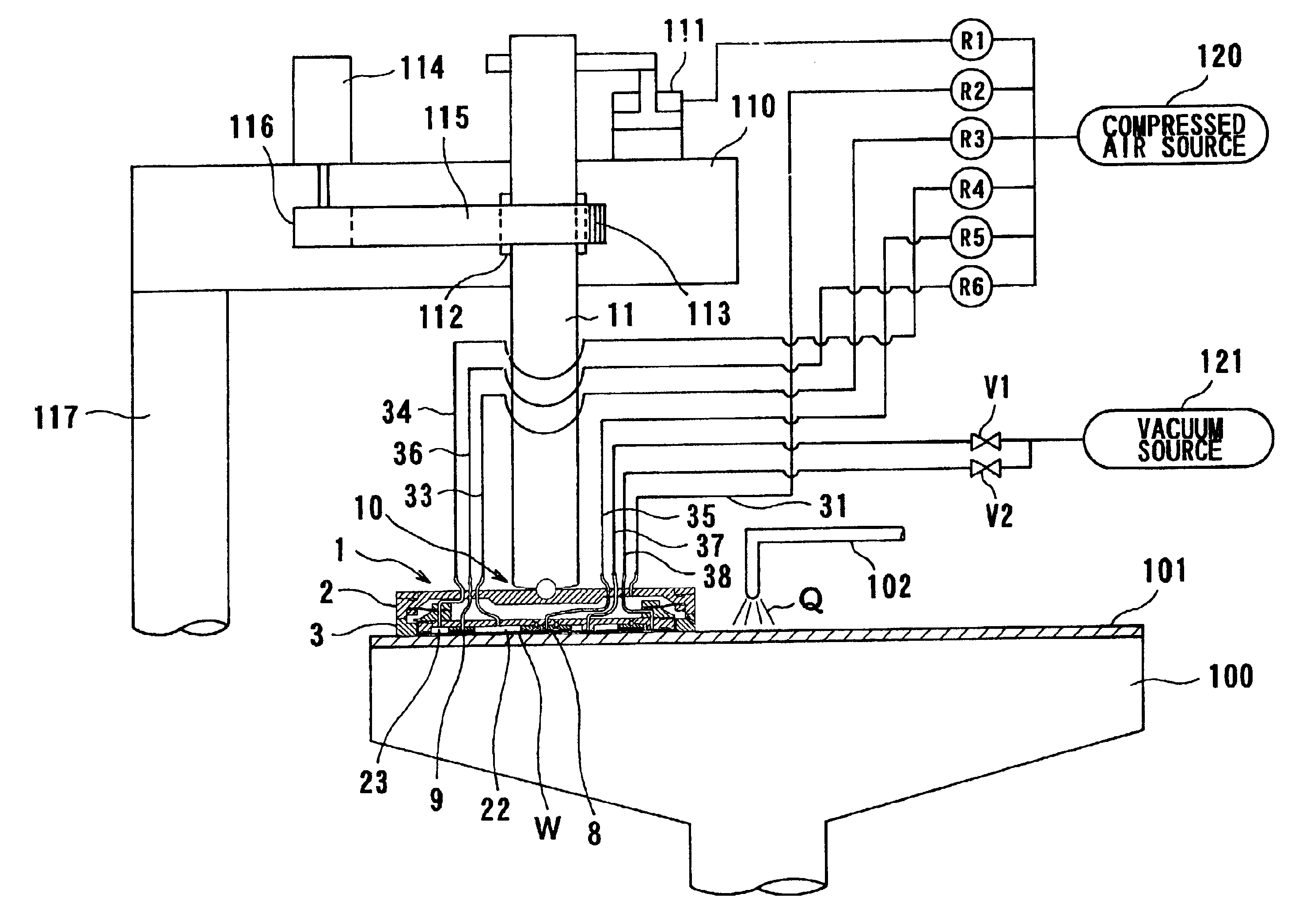
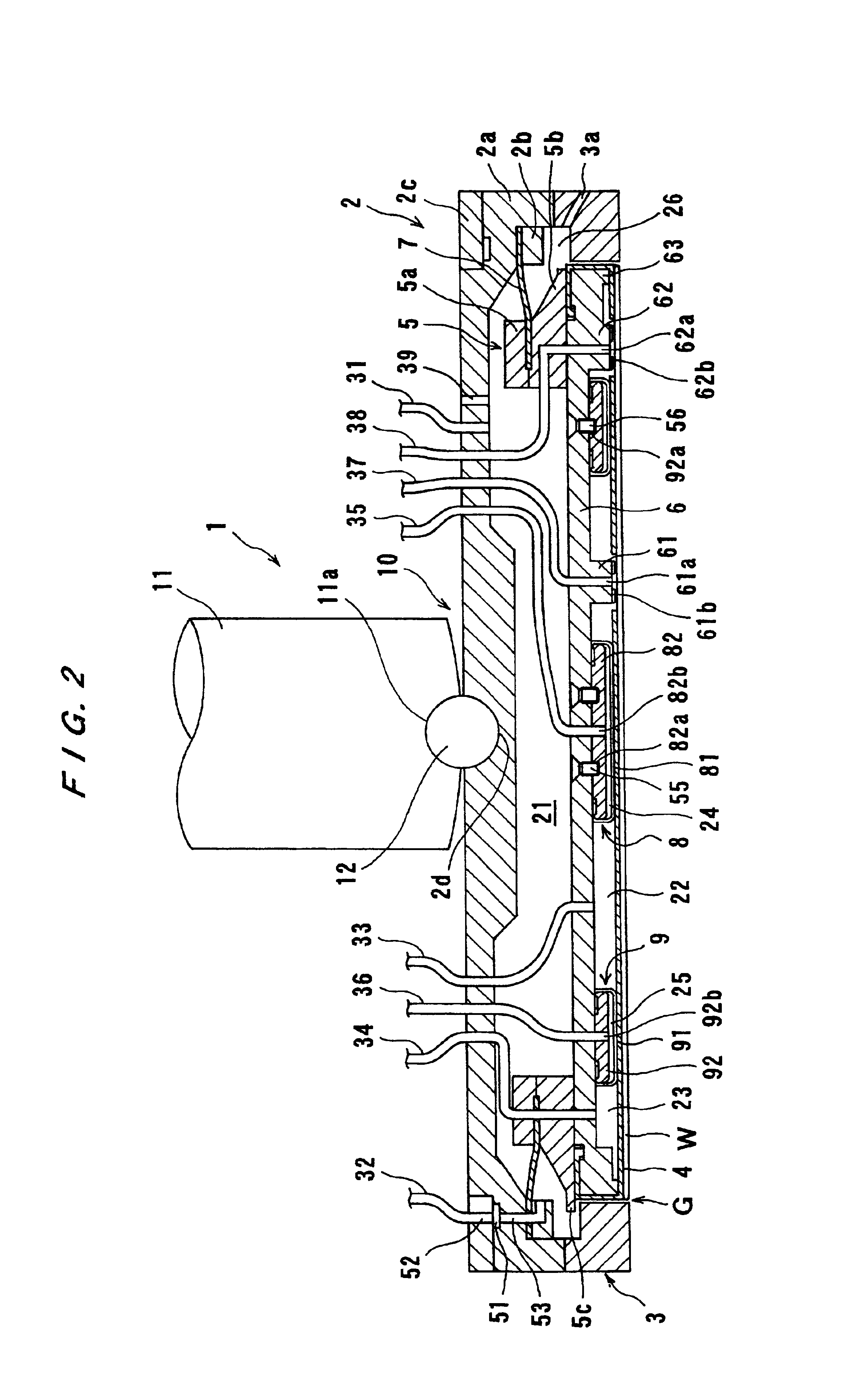
A polishing apparatus according to the present invention will be described below with reference to FIGS. 1 through 6.

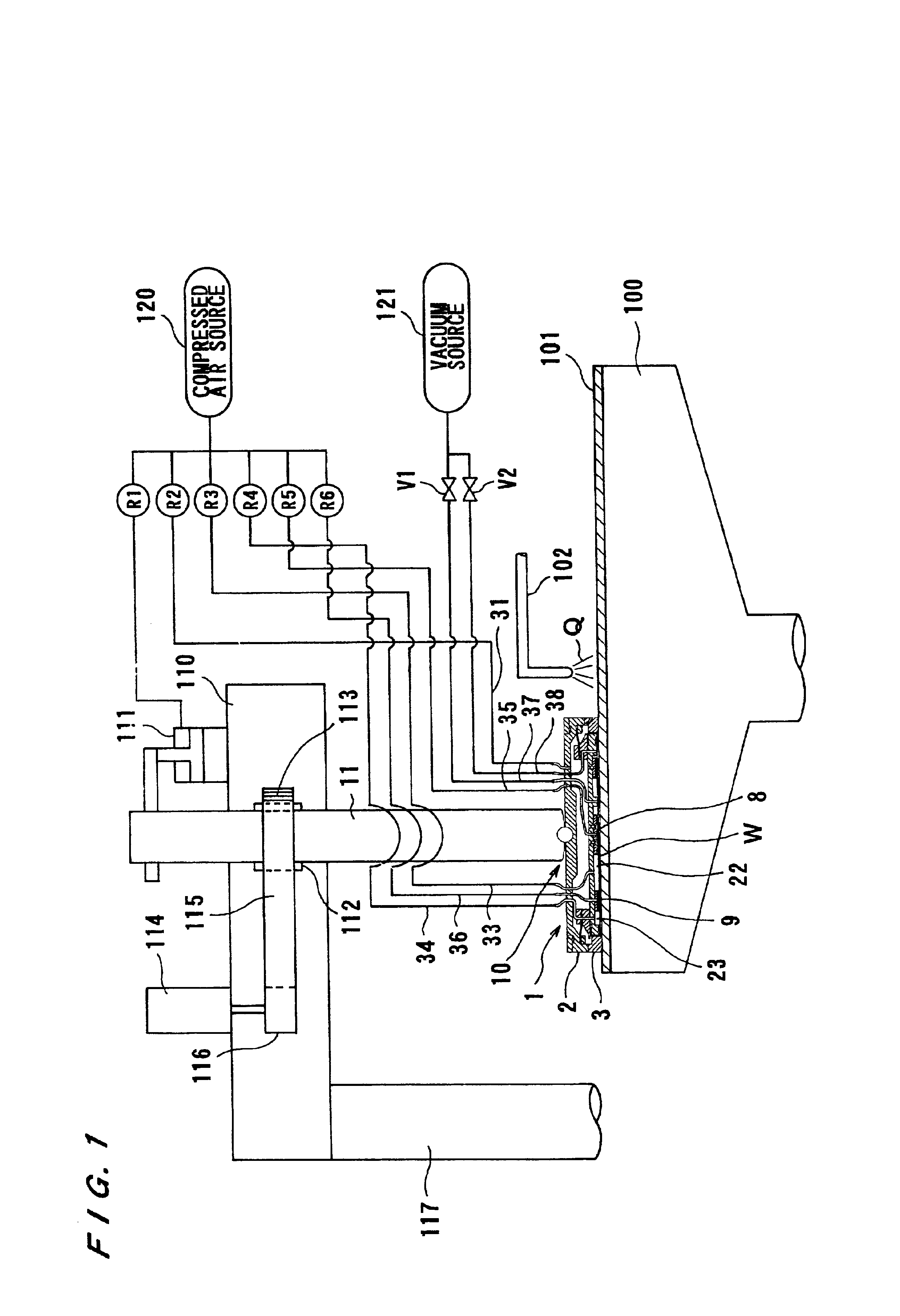
FIG. 1 is a cross-sectional view showing an entire structure of a polishing apparatus having a substrate holding apparatus according to the first embodiment of the present invention. The substrate holding apparatus serves to hold a substrate, such as a semiconductor wafer, to be polished and to press the substrate against a polishing surface of a polishing table. As shown in FIG. 1, a polishing table 100 is disposed underneath a top ring 1 constituting the substrate holding apparatus according to the present invention, and has a polishing pad 101 attached to an upper surface thereof A polishing liquid supply nozzle 102 is disposed above the polishing table 100 and supplies a polishing liquid Q onto the polishing pad 101 on the polishing table 100.

Various kinds of polishing pads are sold on the market. For example, some of these are SUBA800, IC-1000, and IC-1000 / SUBA40...


PUM


Abstract

The present invention relates to a substrate holding apparatus for holding a substrate to be polished and pressing the substrate against a polishing surface. The substrate holding apparatus comprises a top ring body for holding a substrate, an elastic pad for being brought into contact with the substrate, and a support member for supporting the elastic pad. The substrate holding apparatus further comprises a contact member mounted on a lower surface of the support member and disposed in a space formed by the elastic pad and the support member. The contact member has an elastic membrane for being brought into contact with the elastic pad. A first pressure chamber is defined in the contact member, and a second pressure chamber is defined outside of the contact member. The substrate holding apparatus further comprises a fluid source for independently supplying a fluid into, or creating a vacuum in, the first pressure chamber and the second pressure chamber.

Description

BACKGROUND OF THE INVENTION1. Field of the InventionThe present invention relates to a substrate holding apparatus for holding a substrate to be polished and pressing the substrate against a polishing surface, and more particularly to a substrate holding apparatus for holding a substrate such as a semiconductor wafer in a polishing apparatus for polishing the substrate.2. Description of the Related ArtIn a manufacturing process of a semiconductor device, a thin film is formed on a semiconductor device, and then micro-machining processes, such as patterning or forming holes, are performed. Thereafter, the above processes are repeated to form thin films on the semiconductor device. Recently, semiconductor devices have become more integrated, and structure of semiconductor elements has become more complicated. In addition, the number of layers in multilayer interconnections used for a logical system has been increased. Therefore, irregularities on a surface of the semiconductor device ...

Claims


Application Information

Patent Timeline
Patent Type & Authority Patents(United States)
IPC IPC(8): B24B37/04B24B41/06B24B37/005B24B37/30H01L21/304
CPCB24B41/061B24B37/30H01L21/304
Inventor TOGAWA, TETSUJINOJI, IKUTARONAMIKI, KEISUKEYASUDA, HOZUMIKOJIMA, SHUNICHIROSAKURAI, KUNIHIKOTAKADA, NOBUYUKINABEYA, OSAMUFUKUSHIMA, MAKOTOTAKAYANAGI, HIDEKI
Owner EBARA CORP
Why Eureka
Try Eureka