Silicon penetration device with increased fracture toughness and method of fabrication

a technology of fracture toughness and silicon penetration, which is applied in the direction of transportation and packaging, water-setting substance layered products, vacuum evaporation coating, etc., can solve the problems of actual failure of silicon penetration devices, increase in surface flaws, and inability to strengthen devices through surface modifications, etc., to achieve increase in fracture toughness, increase fracture toughness, and increase fracture toughness

Inactive Publication Date: 2005-02-08
KUMETRIX
View PDF5 Cites 31 Cited by
  • Summary
  • Abstract
  • Description
  • Claims
  • Application Information

AI Technical Summary

Benefits of technology

Another object of the present invention is to provide silicon penetration devices on which a silicon oxide layer was thermally grown from the bulk silicon material of the device substrate and then subsequently removed, resulting in an increase in fracture toughness.
Still another object of the present invention is to provide silicon penetration devices which are coated with a one (1) micrometer nickel film, resulting in an increase in fracture t

Problems solved by technology

Common MEMS fabrication methods, such as bulk etching with potassium hydroxide solution, leave the surface of the penetration device in a roughened state, with resultant increase in surface flaws.
The actual failure of th

Method used


Image

  • Silicon penetration device with increased fracture toughness and method of fabrication
  • Silicon penetration device with increased fracture toughness and method of fabrication

Examples


Embodiment Construction

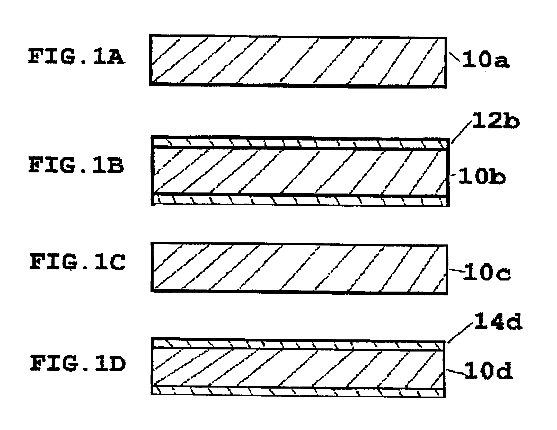
The present invention comprises methods of increasing the fracture toughness of silicon penetration devices. The first method comprises two steps. In the first step, the silicon surface of the device substrate is reacted at elevated temperatures with gaseous materials to form a thick adherent silicon-containing chemical film, for example a silicon oxide or oxynitride, on the silicon substrate surface. In the second step, the chemically-bound silicon film is removed by etching.

FIG. 1A shows a side sectional view of silicon substrate 10a of a previously unprocessed penetration device, that is, a device prior to applying the methods of this invention. The penetration device silicon has been fabricated using standard integrated circuit (IC) and microelectromechanical systems (MEMS) processing technologies, probably including wet etching.

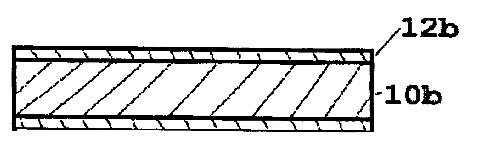
As illustrated in FIG. 1B, an embodiment of the present invention includes a method for strengthening silicon penetration devices by thermally growing a...


PUM

PropertyMeasurementUnit
Temperatureaaaaaaaaaa
Thicknessaaaaaaaaaa
Lengthaaaaaaaaaa

Abstract

A silicon penetration device with increased fracture toughness and method of fabrication thereof are provided. The method comprises strengthening silicon penetration devices by thermally growing a silicon oxide layer on the penetration device and then subsequently stripping the silicon oxide. The method also includes strengthening silicon penetration devices through the sputtering of thin film coatings on the silicon penetration devices.

Description

TECHNICAL FIELDThis invention relates generally to a method for strengthening silicon penetration devices such as needles or probes by increasing fracture toughness.BACKGROUNDIt is well known in the art that silicon is a brittle substance. A penetration device constructed from single crystal silicon must possess a certain degree of mechanical robustness in order to ensure successful use of the needle without accidental fracture of the needle in patients. The device may have an interior channel (a hollow penetration device through which fluids can pass for sampling or injection) or it may be solid (for use as a lancet or probe). Integrated circuit and MEMS (microelectromechanical systems) technologies are used to fabricate these silicon penetration devices. Common MEMS fabrication methods, such as bulk etching with potassium hydroxide solution, leave the surface of the penetration device in a roughened state, with resultant increase in surface flaws. The actual failure of the silicon...

Claims


Application Information

Patent Timeline
IPC IPC(8): C23C14/16C23C14/02
CPCC23C14/021C23C14/165C23C14/024Y10T428/265
Inventor SMART, WILSONSUBRAMANIAN, KUMARORLOFF, EUGENE
Owner KUMETRIX
Why Eureka
Try Eureka