Method for the production and configuration of organic field-effect transistors (OFET)

a field-effect transistor and organic technology, applied in the direction of printing, thermoelectric devices, other printing apparatuses, etc., can solve the problems of significant reduction in the performance of the ofet obtained, and achieve the effect of cost-effective and greater performan

Inactive Publication Date: 2005-02-08
POLYIC GMBH & CO KG
View PDF18 Cites 72 Cited by
  • Summary
  • Abstract
  • Description
  • Claims
  • Application Information

AI Technical Summary

Benefits of technology

Therefore, it is an object of the invention to provide a cost-effective method, suitable for mass production, for producing and patterning OFETs, and an OFET which exhibits greater performance, because it is equipped with more patterned layers.

Problems solved by technology

The lack of patterning of the other layers, such as the semiconducting layer and the insulating layer made of functional polymers, leads to a significant reduction in performance of the OFETs obtained, but it is dispensed with for cost reasons.

Method used


Image

  • Method for the production and configuration of organic field-effect transistors (OFET)
  • Method for the production and configuration of organic field-effect transistors (OFET)
  • Method for the production and configuration of organic field-effect transistors (OFET)

Examples


Embodiment Construction

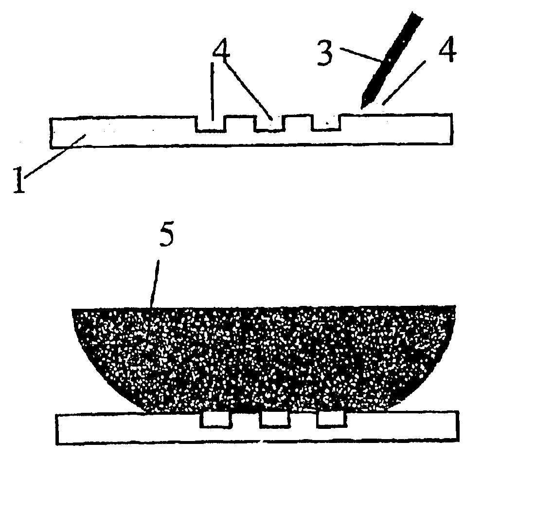
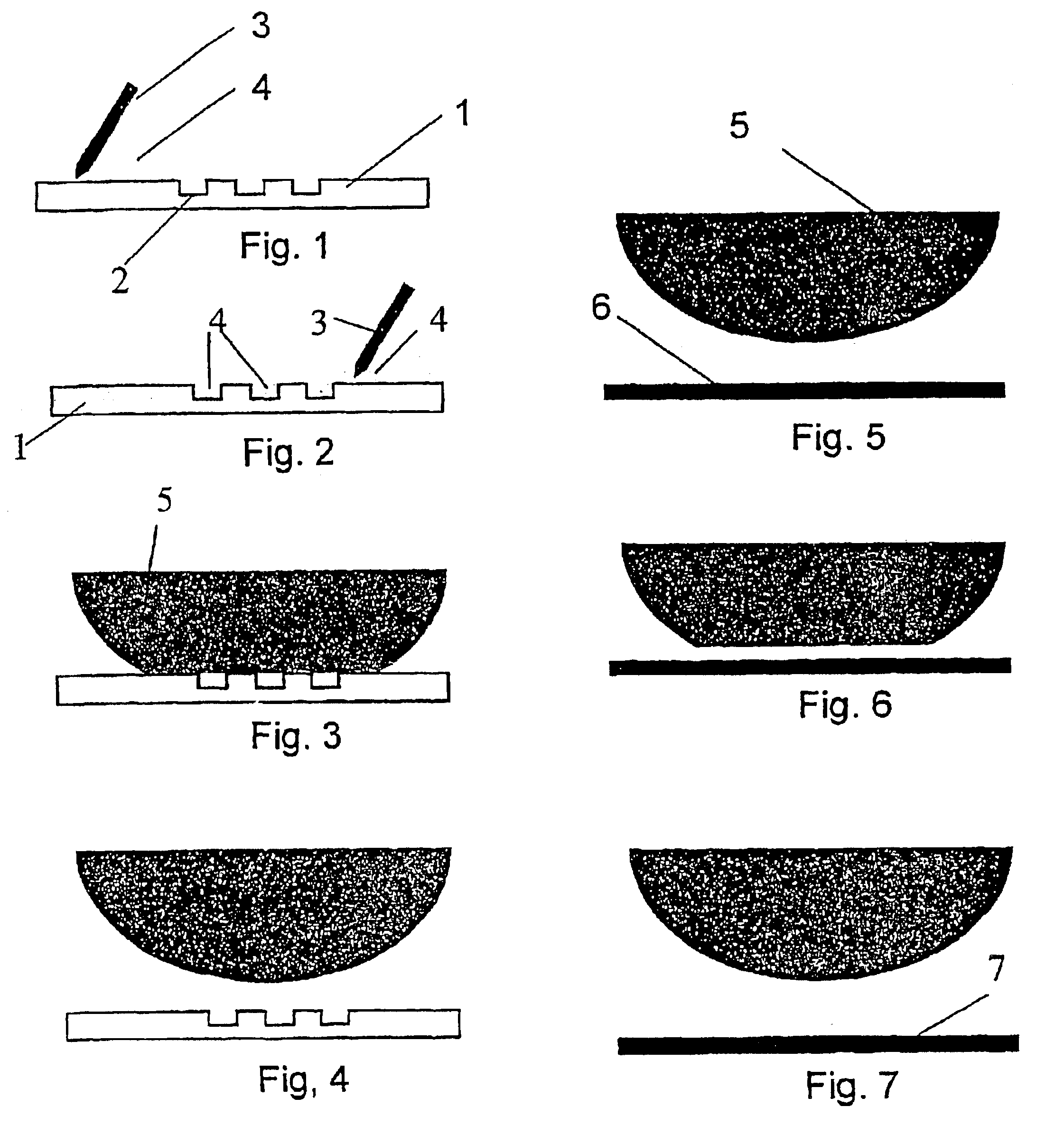
Firstly, the block 1 with the negatives 2 of the structure to be applied is shown in FIG. 1. Before the negative imprinting, it is possible to discern a doctor blade 3, which applies the functional polymer 4 along the block by blade. In FIG. 2, the negative 2 of the block is filled with functional polymer 4 and the doctor blade continues to slide precisely with the remainder of polymer on the block 1, which can rotate, for example. FIG. 3 reveals the large pad roll 5, which takes up the finished patterned functional polymer 4 from the block 3 and (cf. FIGS. 4 to 7) images it onto a substrate 6. The finished applied and patterned OFET 7 can be seen in FIG. 7.

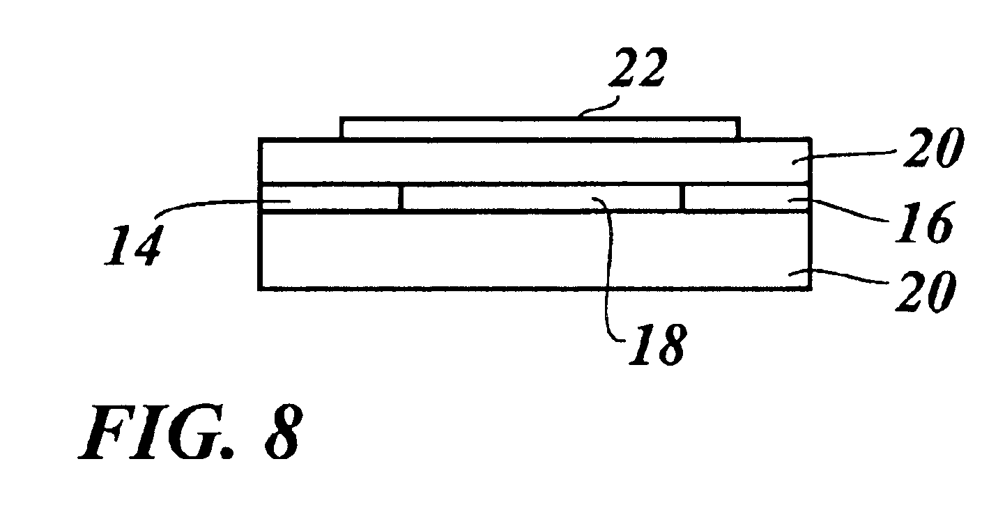
An OFET as described above is shown in more detail in FIG. 8 wherein the OFET 10 includes a substrate 12, a source 14, a drain 16, a semiconductor layer 18, an insulator layer 20 and a conductor layer 22.

The invention provides a cost-effective and precise method for producing and patterning OFETs by utilizing the solubility of at...


PUM


Abstract

The invention relates to an economical and precise method for the production and configuration of an organic field-effect transistor (OFET) whereby the solubility of at least one functional polymer of an OFET is utilized to such a degree, that the functional polymer is deposited on the OFET, or a substrate, by means of a conventional printing process as for a color.

Description

BACKGROUND OF THE INVENTIONThe invention relates to a method for producing and patterning organic field-effect transistors (OFETs).Polymeric integrated circuits based on OFETs are used for microelectronic mass applications and disposal products such as identification and product tags. A tag is e.g. an electronic bar code of the kind provided on merchandise or on luggage. In this case, the excellent operating behavior of silicon technology can be dispensed with, but by the same token low producing costs and mechanical flexibility should be ensured. The devices such as e.g. electronic bar codes are typically disposable products and are of interest economically only if they are produced in inexpensive processes.To date, owing to the production costs, only the conductor layer of the OFET has been patterned since the patterning can only be realized using a two-stage process (“lithography method” cf. in this respect Applied Physics Letters 73(1), 1998, p. 108.110 and Mol. Cryst. Liq. Crys...

Claims


Application Information

Patent Timeline
Patent Type & Authority Patents(United States)
IPC IPC(8): H01L51/40H01L51/05B41M1/40H01L21/00H01L21/288H01L21/336H01L29/786H01L35/24H01L51/00
CPCH01L51/0004H01L51/0516H01L51/0021H10K71/13H10K71/60H10K10/468
Inventor BERNDS, ADOLFCLEMENS, WOLFGANGFIX, WALTERROST, HENNING
Owner POLYIC GMBH & CO KG
Why Eureka
Try Eureka