

Method for fabricating MOS transistors
a technology of metal oxide semiconductors and transistors, which is applied in the direction of semiconductor devices, basic electric elements, electrical equipment, etc., can solve the problems of reducing the reliability of the semiconductor device, gradual increase of degradation of the characteristics of the device, etc., and achieves the effect of avoiding degradation of the device characteristics and increasing the junction capacitan
- Summary
- Abstract
- Description
- Claims
- Application Information
AI Technical Summary
Benefits of technology
Problems solved by technology
Method used
Image

Examples
Embodiment Construction
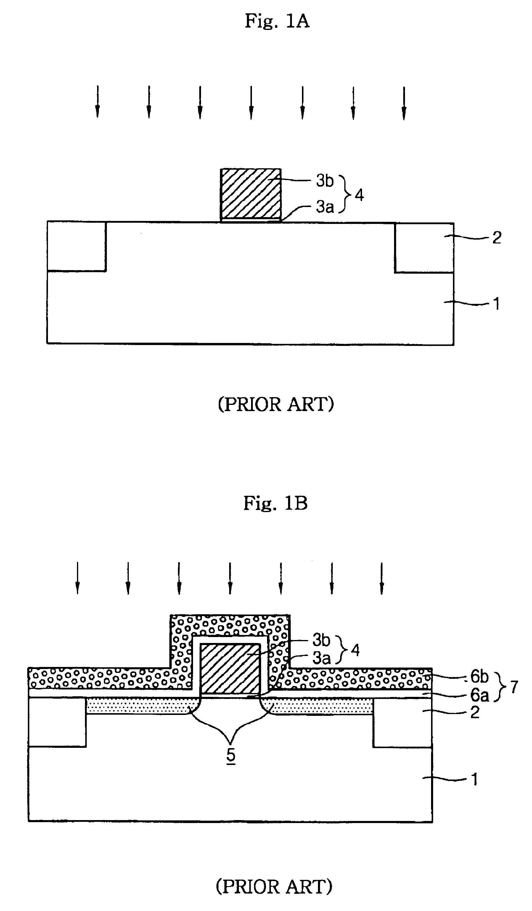
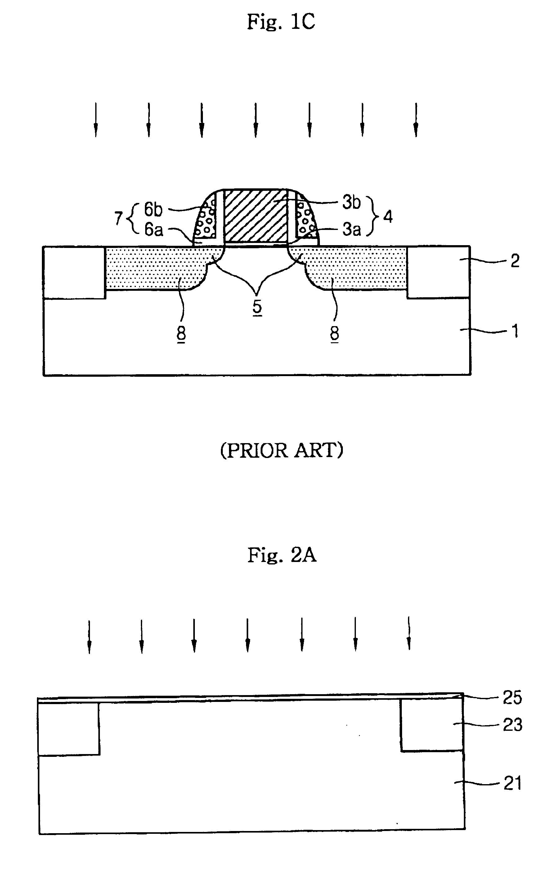
Hereinafter, a preferred embodiment of the present invention will be described with reference to the accompanying drawings. In the following description and drawings, the same reference numerals are used to designate the same or similar components, and so repetition of the description of the same or similar components will be omitted.
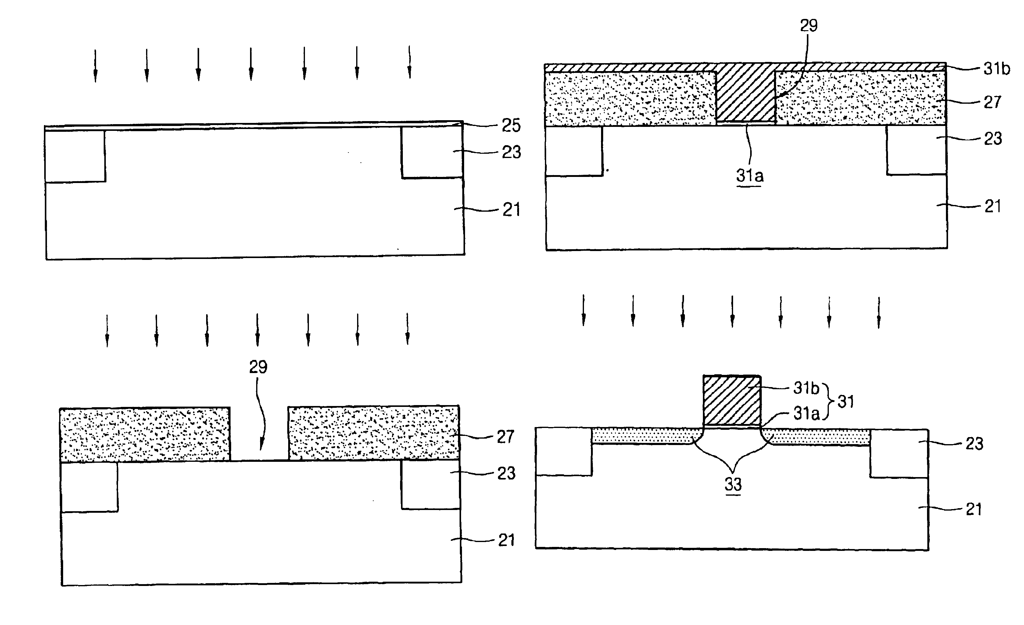
FIGS. 2A to 2E are end views showing a fabricating method of MOS transistors of an embodiment of the present invention according to every processes.
Referring to the FIG. 2A, a buffer oxide layer 25 is formed on a semiconductor substrate 21 having a trench type isolation layer 23. Then, ion implantations for well formation and field stop formation are successively conducted to an active region of the substrate 21 through the buffer oxide layer 25.
Referring to the FIG. 2B, the buffer oxide layer is removed and a sacrificial layer 27 composed of a chemical vapor deposition (CVD) oxide layer is formed on the semiconductor substrate 21 so as to have a thickn...
PUM
 Abstract
Description
Claims
Application Information