

On-chip waveguide feeder for millimeter wave ICS and feeding methods, and multiple input and output millimeter wave transceiver system using same
a millimeter wave ics and feed technology, applied in waveguide mouths, instruments, reradiation, etc., can solve the problem of not being able to implement the rear via in a silicon standard process
- Summary
- Abstract
- Description
- Claims
- Application Information
AI Technical Summary
Benefits of technology
Problems solved by technology
Method used
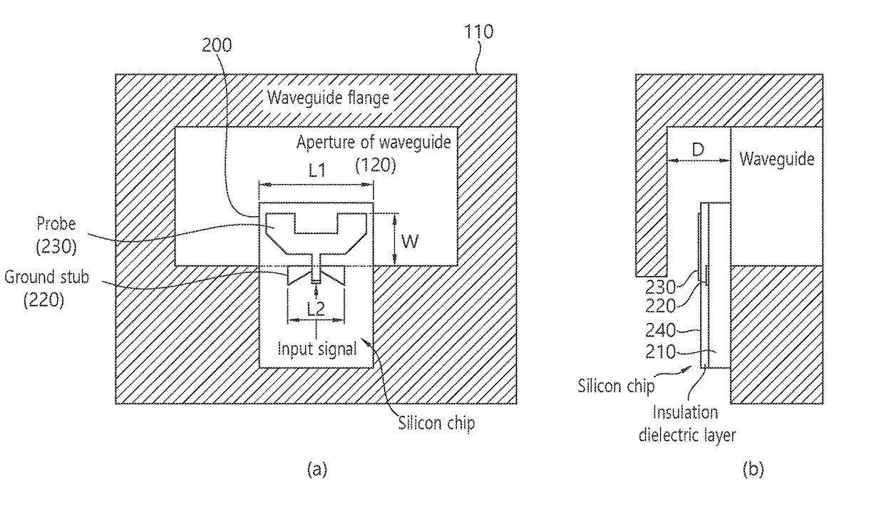
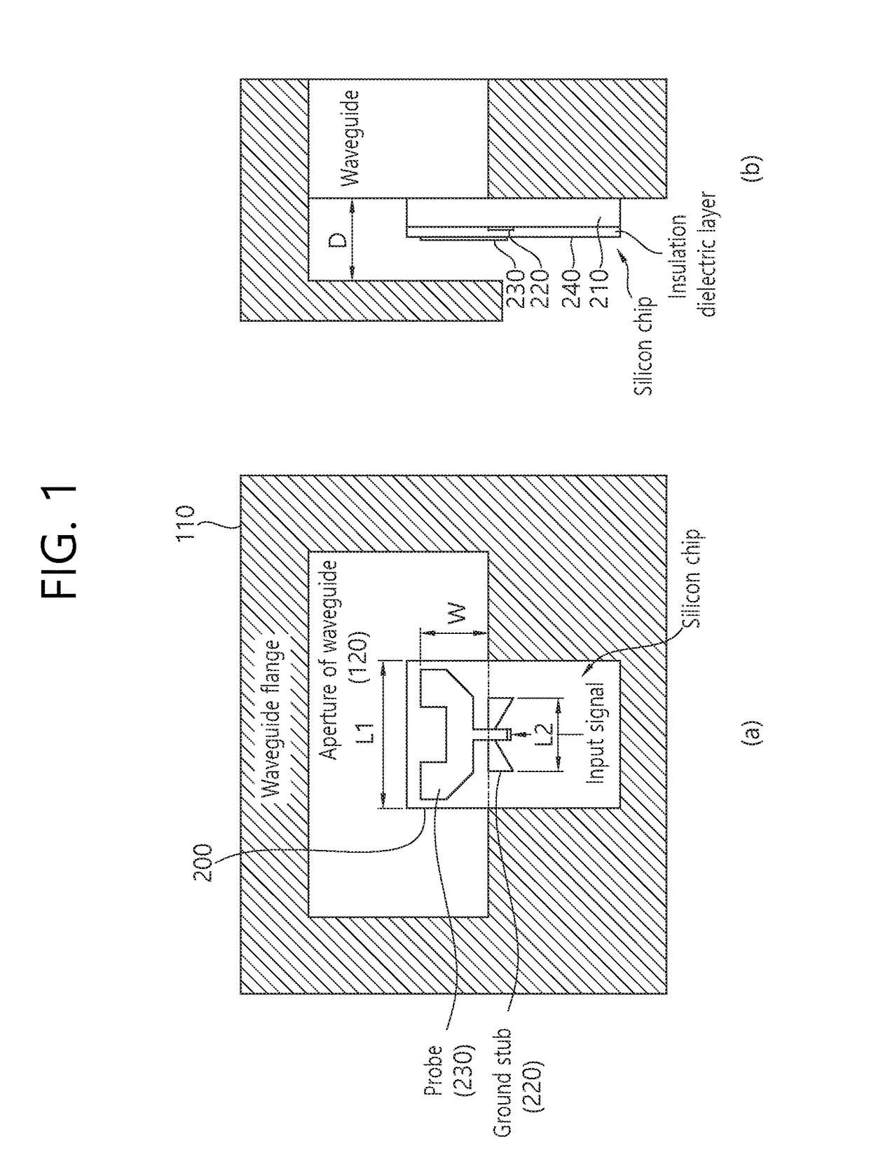
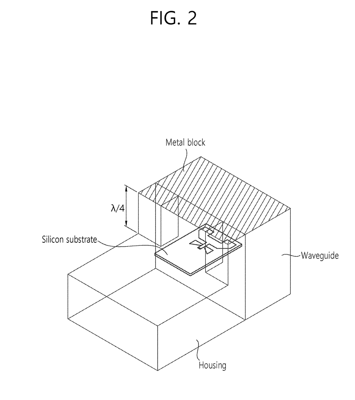
Image

Examples
Embodiment Construction
[0040]Rather, these example embodiments are provided so that this disclosure will be thorough and complete, and will fully convey the scope of the present inventive concept to those skilled in the art.
[0041]However, the embodiment is not limited to the specific embodiment, but the embodiment includes all modifications, equivalents, and substitutes belonging to the technical scope of the embodiment without departing from the spirit of the embodiment.
[0042]It will be understood that, although the terms first, second, third etc. may be used herein to describe various elements, these elements should not be limited by these terms. These terms are used to distinguish one element from another. Thus, a first element discussed below could be termed a second element without departing from the teachings of the present inventive concept. As used herein, the term “and / or” includes any and all combinations of one or more of the associated listed items.
[0043]In addition, when a component is referr...
PUM
 Abstract
Description
Claims
Application Information