Image-forming apparatus and method of manufacturing the same

a technology of image-forming apparatus and manufacturing method, which is applied in the direction of discharge tube luminescnet screen, discharge tube, instrument, etc., can solve the problems of degrading the electron source in the vicinity, affecting the normal operation of display, and the surface creepage may occur via the surface of the supporting frame, so as to prevent the concentration of an electric field and the occurrence of surface creepage , the effect of reducing the damage caused by discharg

Inactive Publication Date: 2005-02-08
CANON KK
View PDF9 Cites 23 Cited by
  • Summary
  • Abstract
  • Description
  • Claims
  • Application Information

AI Technical Summary

Benefits of technology

[0010]Therefore, with the foregoing in mind, it is an object of the present invention to provide a highly reliable image-forming apparatus that prevents the concentration of an electric field and the occurrence of surface creepage caused by an apparatus configuration, and remarkably reduces damage caused by discharge so as to prevent breakage of the apparatus even in the case where discharge occurs in the apparatus using an electron source, and a method of manufacturing the same.

Problems solved by technology

Particularly, in the case where spacer members are disposed in the image-forming apparatus for the purpose of keeping a predetermined interval between the rear plate and the face plate and of supporting the plates against an atmospheric pressure, and in the case where getter members are disposed for the purpose of maintaining a high vacuum state, an electric field is likely to be concentrated in the vicinity of these spacer members and getter members, which may cause discharge.
Furthermore, in the structure in which a supporting frame is disposed in the vicinity of anode electrodes so as to miniaturize the image-forming apparatus, surface creepage may occur via the surface of the supporting frame.
The above-mentioned discharge suddenly occurs during an image display, which may not only disturb an image but also remarkably degrade the electron source in the vicinity of a discharge portion.
Accordingly, there is a possibility that a display may not be conducted normally.

Method used


Image

  • Image-forming apparatus and method of manufacturing the same
  • Image-forming apparatus and method of manufacturing the same
  • Image-forming apparatus and method of manufacturing the same

Examples


example 1

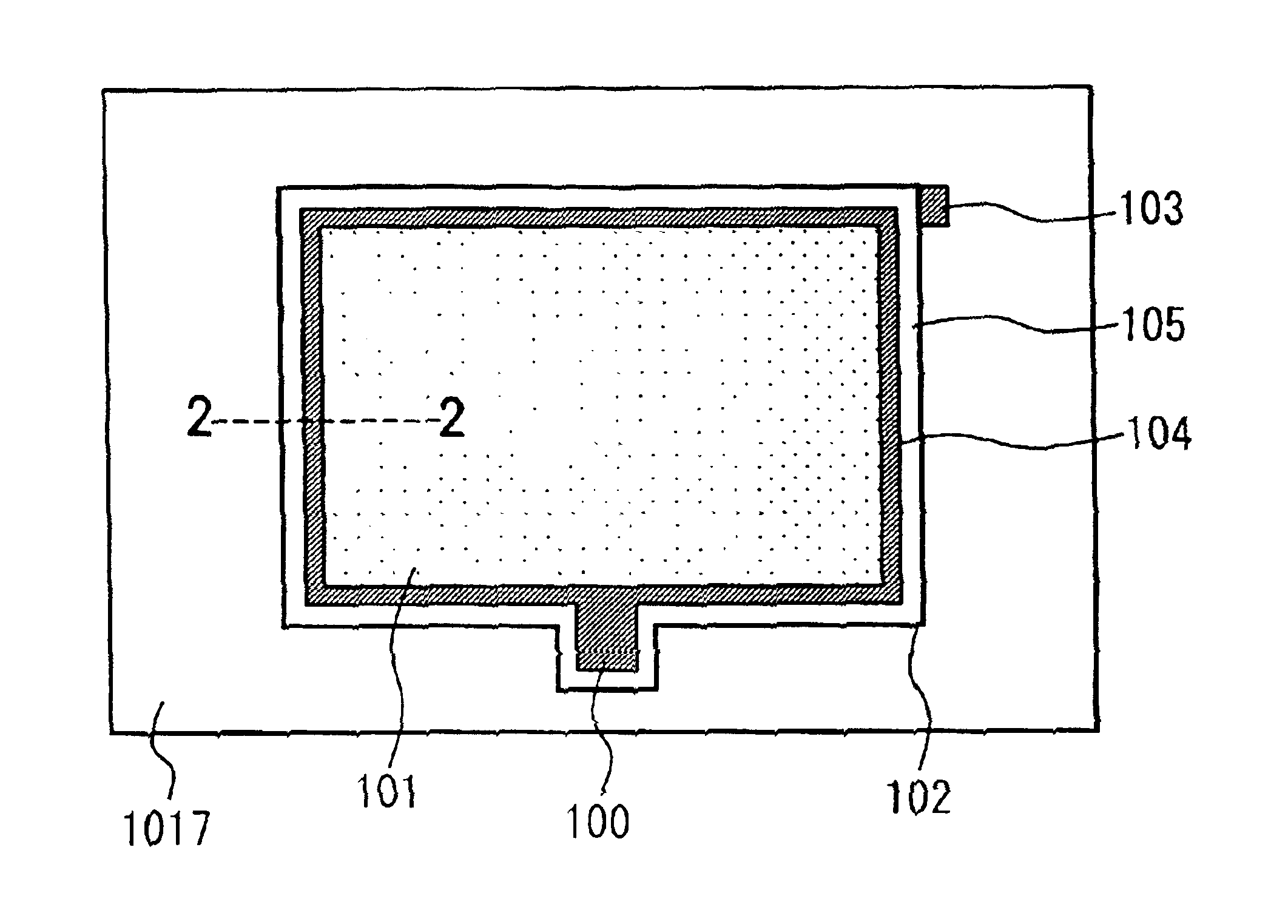
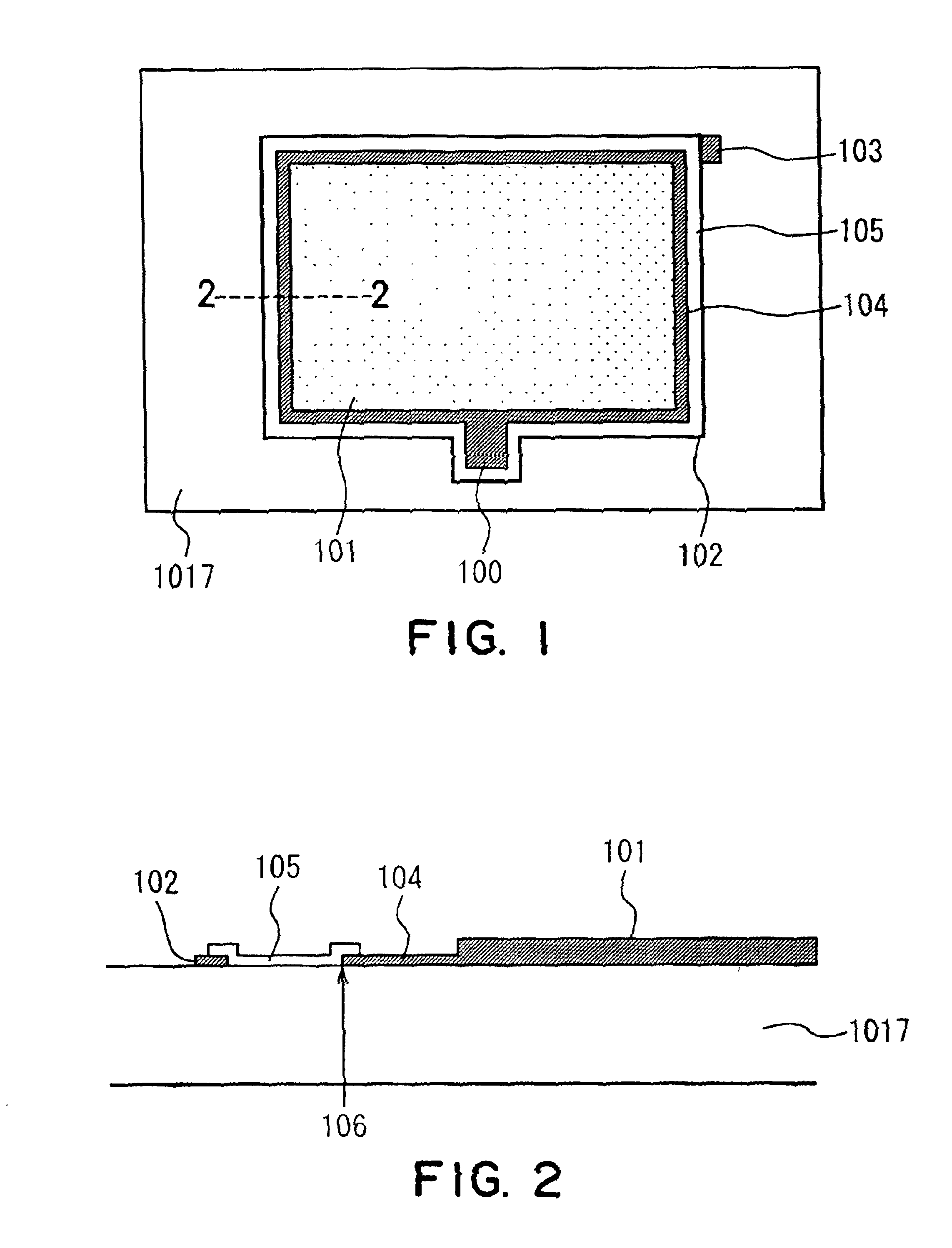
[0083]In the present example, two kinds of resistant films are formed between an image display region and an electroconductive member. FIG. 9 is a cross-sectional view showing the resistant films. Herein, reference numeral 1017 denotes a face plate substrate, 1019 denotes a metal back, 102 denotes an electroconductive member, 104 denotes a first resistant film (first resistant member), 105 denotes a second resistant film (second resistant member), 106 denotes a resistance border portion, and 401 denotes phosphors and a black matrix. The metal back 1019 and the phosphors and the black matrix 401 constitute an image display region.

[0084]First, as the first resistant film 104, WGeN (nitride of tungsten and germanium) was formed to a film with a thickness of about 250 [nm]. The first resistant film 104 was formed by sputtering for 20 minutes under the conditions of a total pressure of 1.5 [Pa], an Ar flow rate of 50 [sccm], an N2 flow rate of 5 [sccm], and a W input power of 239 [W], an...

example 2

[0086]In the present example, a first resistant film (first resistant member) was made of ITO. FIG. 10 shows a cross-sectional view thereof. Reference numeral 1017 denotes a face plate substrate, 1019 denotes a metal back, 102 denotes a conductive member, 104 denotes a first resistant film, 105 denotes a second resistant film, 106 denotes a resistance border portion, and 401 denotes phosphors and a black matrix. The metal back 1019 and the phosphors and the black matrix 401 constitute an image display region.

[0087]In the present example, an ITO film was also formed in the image display region, and the first resistant film 104 was continuously formed (104 in the figure) at the same time under the same conditions as shown in FIG. 10. Furthermore, in the present example, the ITO film was formed before forming the electroconductive member 102 and a high voltage applying terminal abutting portion (not shown). The ITO film has a thickness of about 200 [nm], and a sheet resistance of about...

example 3

[0089]In the present example, WGeN is used for a resistant film, and sputtering conditions are varied, whereby the resistances of the first and second resistant films are changed. The cross-sectional structure in the present example is the same as that in Example 1 (FIG. 9). Regarding the film-formation conditions, only an input power is changed, and the remaining conditions are a total pressure of 1.5 [Pa], an Ar flow rate of 50 [sccm], an N2 flow rate of 5 [sccm], and a Ge electric power of 600 [W]. In forming the first resistant film, a W (tungsten) input power was set to 230 [W] to obtain a sheet resistance of about 4×10⁹ [Ω / square]. In forming the second resistant film, a W (tungsten) input power was set to 180 [W] to obtain a sheet resistance of about 2×10¹² [Ω / square].

[0090]An image-forming apparatus was formed by using the above-mentioned face plate. The same effects as those in Example 1 were obtained. In this case, the material of the first resistant film is the same as th...


PUM


Abstract

An image-forming apparatus of the present invention includes: a vacuum container constituted by disposing in opposition to each other a rear plate with an electron source formed thereon, and a face plate having an image display region provided with at least phosphors for being irradiated with electrons emitted from the electron source to form an image and anodes disposed on the phosphors; anode potential supplying means for supplying an electric potential higher than that of the electron source to the anode; at least one electroconductive member provided at a site outside of the image display region on an inner surface of the face plate; potential supplying means for supplying to the electroconductive member an electric potential at a level between a lowest electric potential of those which are applied to the electron source and an electric potential applied to the anode; first and second resistant members electrically connected between the anode and the electroconductive members, having resistances higher than that of the anode and having different resistances from each other, wherein the anode, the first resistant member, the second resistant member, and the electroconductive member are electrically connected in series.

Description

[0002]This application is a division of application Ser. No. 09 / 903,712, filed Jul. 13, 2001, now U.S. Pat. No. 6,509,691 B2, issued Jan. 21, 2003.BACKGROUND OF THE INVENTION[0003]1. Field of the Invention[0004]The present invention relates to an image-forming apparatus such as a display apparatus using an electron beam, and a method of manufacturing the same.[0005]2. Related Background Art[0006]Conventionally, as an image-forming apparatus using electron-emitting devices, a plane type electron beam display panel is known in which an electron source substrate with a number of cold cathode devices formed thereon and an anode substrate provided with anode electrodes and phosphors are opposed to each other in parallel, and an inside thereof is exhausted to a vacuum. For example, U.S. Pat. No. 5,066,883 and the like disclose such an image-forming apparatus using surface conduction electron-emitting devices. A plane type electron beam display panel using surface conduction electron-emitt...

Claims


Application Information

Patent Timeline
Patent Type & Authority Patents(United States)
IPC IPC(8): H01J29/00H01J29/08H01J29/92H01J29/02H01J29/28H01J31/12
CPCH01J29/085H01J29/92H01J31/127H01J2329/92H01J2201/3165
Inventor YAMAZAKI, KOJIONISHI, TOMOYA
Owner CANON KK
Why Eureka
Try Eureka