
Dielectric ceramic, method of producing the same, and monolithic ceramic capacitor

a monolithic ceramic and dielectric ceramic technology, applied in the field of dielectric, can solve the problems of reducing reliability, deteriorating capacitance temperature characteristics, and insufficiently meeting the demands of the market, and achieve the effect of enhancing reliability, easy and secure production

Active Publication Date: 2005-02-08
MURATA MFG CO LTD
View PDF10 Cites 33 Cited by
  • Summary
  • Abstract
  • Description
  • Claims
  • Application Information

AI Technical Summary

Benefits of technology

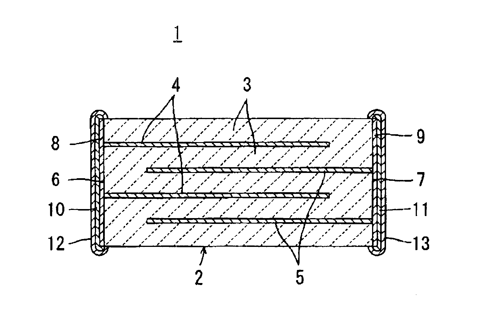
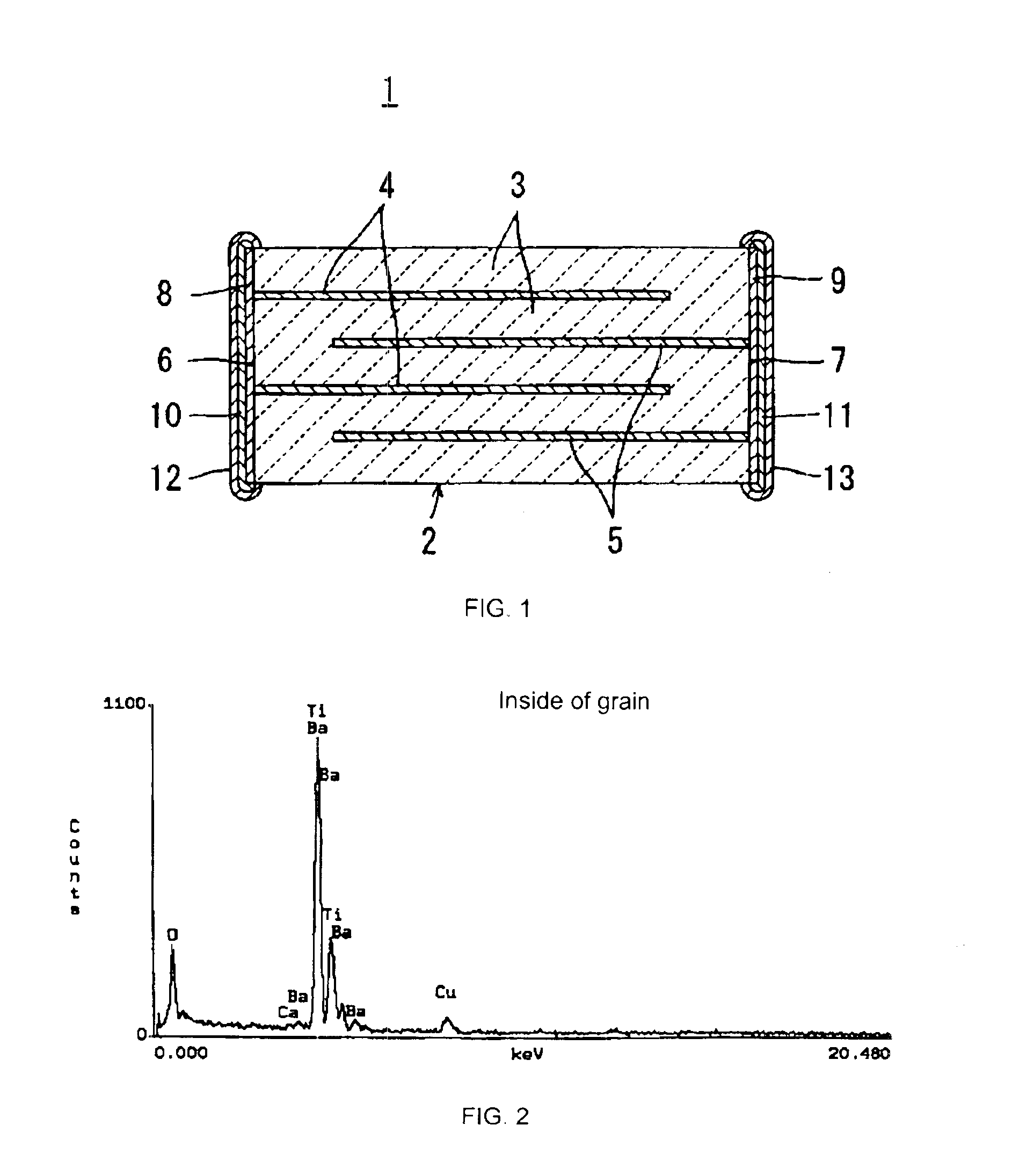
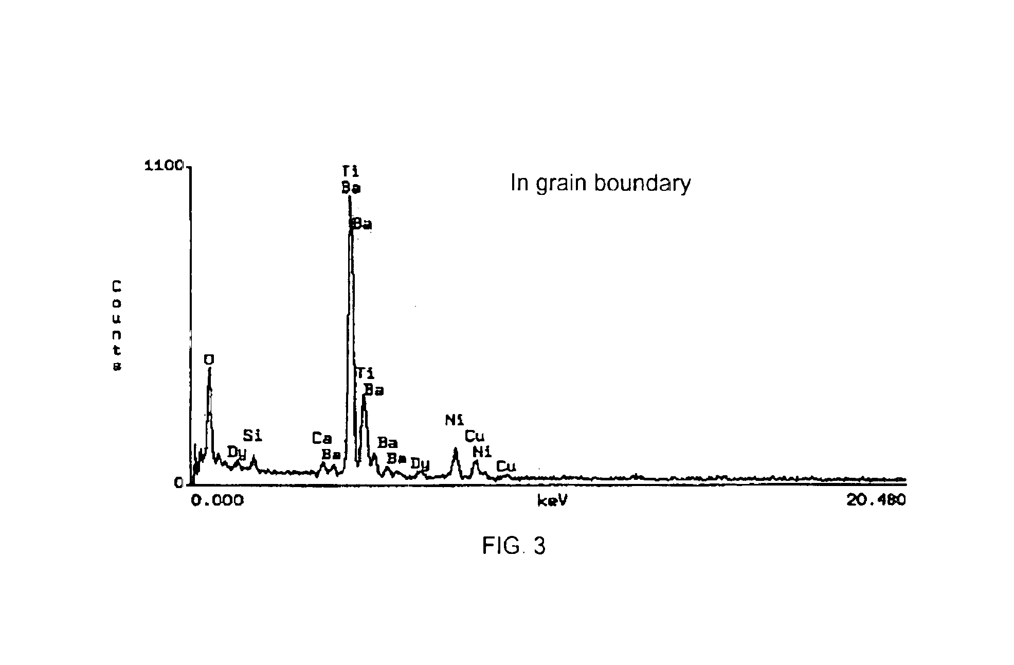
According to the present invention, there is provided a dielectric ceramic which includes, in composition, a perovskite-type compound having the general formula ABO3 in which A represents Ba and Ca, or Ba, Ca and Sr, and B represents Ti or Ti and at least one of Zr and Hf which is substituted for a part of the Ti, and an additive component containing Si, R and M, in which R represents at least one of La, Ce, Pr, Nd, Sm, Eu, Gd, Tb, Dy, Ho, Er, Tm, Yb, Lu and Y, and M represents Mn, Ni, Co, Fe, Cr, Cu, Mg, Al, V, Mo and W, the dielectric ceramic having crystal grains and crystal grain boundaries between the crystal grains, the additive component not being solid-dissolved and, moreover, the major component existing in at least about 90% of the cross-section of each of the crystal grains of at least about 85% of all of the crystal grains, and at least the Ba, Ca, Ti, Si, R and M being at at least about 85% of the analytical points in the crystal grain boundaries. Even if the thickness of a dielectric ceramic layer formed of the dielectric ceramic is reduced, the dielectric ceramic layer has a high reliability. Also, the capacitance—temperature characteristic is superior and the dielectric constant is high. Accordingly, a monolithic ceramic capacitor having a high reliability and a superior capacitance—temperature characteristic can be realized by forming the dielectric ceramic layers of a monolithic ceramic capacitor by using the dielectric ceramic. In addition, the size of the monolithic ceramic capacitor can be reduced, and the capacitance thereof is increased, due to the reduction of the thickness of the dielectric ceramic layer.
Preferably, the formula Cag / Tig<Cab / Tib is established in the dielectric ceramic of the present invention, in which Cag is the amount of Ca, and Tig is the amount of Ti contained in the crystal grains, and Cab is the amount of Ca, and Tib is the amount of Ti contained in the crystal grain boundaries. Thereby, the reliability can be more enhanced.
Preferably, the concentrations on an element basis of the R and the M in the additive component are in the ranges of about 0.05 to 1.5 moles and about 0.1 to 2 moles, respectively, based on 100 moles of the major component. Thereby, the dielectric constant, the capacitance—temperature characteristic, and the reliability can be further enhanced.

Problems solved by technology

However, when the thickness of a dielectric ceramic layer is reduced, and specifically in the case in which the thickness is less than 5 μm, especially less than 3 μm, the capacitance-temperature characteristic and the reliability of the dielectric ceramic do not sufficiently meet the demands in the market.
Moreover, problems occur in that with the thickness of a dielectric ceramic layer being reduced, the capacitance—temperature characteristic is deteriorated, and also, the reliability is reduced.
Thus, problems occur in that for a dielectric ceramic layer of which the thickness is reduced, the capacitance—temperature characteristic and the reliability can not be ensured.
Moreover, if the thickness of a dielectric ceramic layer is decreased and the DC rated voltage is set at the same value as that before the reduction of the thickness, the electric field strength applied per dielectric ceramic layer is increased, and thus, the reliability is remarkably deteriorated.

Method used


Image

  • Dielectric ceramic, method of producing the same, and monolithic ceramic capacitor
  • Dielectric ceramic, method of producing the same, and monolithic ceramic capacitor
  • Dielectric ceramic, method of producing the same, and monolithic ceramic capacitor

Examples


experimental examples

Experimental Example 1

In Experimental Example 1, (Ba0.95Ca0.05)TiO3 was used as major component having the general formula ABO3, which contains Ba, Ca and Ti. As additive components, BaCO3, CaCO3, TiO2, SiO2, Dy2O3 and NiO were used, as shown in Table 1. Sample 1 as an embodiment of the present invention, and Samples 2-1 and 2-2 as comparative examples were evaluated.

1. Preparation of Powdery Dielectric Ceramic Raw Material

(1) Sample 1

First, BaCO3, CaCO3, and TiO2 were prepared as starting materials for the major component ABO3, and weighed out so that the composition of (Ba0.95Ca0.05)TiO3 could be produced. Subsequently, the raw materials were mixed for 72 hours with a ball mill and heat-treated at 1150° C. Thus, (Ba0.95Ca0.05)TiO3 was produced. The synthetic degree of this major component of ABO3 was evaluated based on the crystallographic axial ratio c / a of a tetragonal system. The axial ratio c / a was very high, i.e., 1.0101, as shown in Table 1. The average grain size was 0.3 μm...

experimental example 2

In Experimental Example 2, preferred ranges of the amounts of Ca and Ti in dielectric ceramics according to the present invention were determined. The ratio Cag / Tig and the ratio Cab / Tib in which Cag and Tig represent the amounts of Ca and Ti in crystal grains, and Cab and Tib represent the amounts of Ca and Ti in crystal grain boundaries (including a triple point), can be easily controlled by changing the ratio of the amounts of Ca and Ti, that is, the ratio Ca / Ti, in the major component raw material, and also, by changing the ratio the mounts of Ca and Ti, that is, the ratio Ca / Ti, in the additive component raw material.

Table 4 for Experimental Example 2 corresponds to Table 1 for Experimental Example 1. Table 4 shows the compositions and the crystallographic axial ratios c / a of the major components ABO3 and the compositions of calcined materials formed as the additive components in samples prepared in Experimental Example 2.

TABLE 4Crystallo-graphicSam-axial ratioplec / a of majornu...

experimental example 3

Experimental Example 3 was carried out to evaluate a preferred range of the concentration of Ca in crystal grains contained in the dielectric ceramic.

Table 6 corresponds to Table 1 for Experimental Example 1. Table 6 shows the compositions and the crystallographic axial ratio c / a of the major components ABO3 and the compositions of the calcined materials formed as the additive components in samples prepared in Experimental Example 3.

TABLE 6Crystallographicaxial ratio c / a ofSampleMajor componentmanor componentAdditive componentnumberABO3ABO3(calcined material)*11 100BaTiO31.00991.1Ba—0.2Ca—1.0Ti—1.4Si—1.0Dy—1.0Mn—0.5Ni—0.5Mg—O12100(Ba0.99Ca0.01)TiO31.01021.1Ba—0.2Ca—1.0Ti—1.4Si—1.0Dy—1.0Mn—0.5Ni—0.5Mg—O13100(Ba0.89Ca0.10Sr0.01)TiO31.00971.0Ba—0.1Ca—1.2Ti—1.2Si—1.0Dy—1.0Mn—0.5Ni—0.5Mg—O14100(Ba0.80Ca0.20)(Ti0.995Hf0.005)O31.00951.0Ba—0.1Ca—1.2Ti—1.2Si—1.0Dy—1.0Mn—0.5Ni—0.5Mg—O15100(Ba0.79Ca0.21)TiO31.00941.0Ba—0.2Ca—1.0Ti—1.4Si—1.0Dy—1.0Mn—0.5Ni—0.5Mg—O

As shown in Table 6, powdery die...


PUM

PropertyMeasurementUnit
thicknessesaaaaaaaaaa
thicknessaaaaaaaaaa
thicknessaaaaaaaaaa

Abstract

A dielectric ceramic includes, in composition, a perovskite-type compound having the general formula ABO3 containing Ba, Ca and Ti, and an additive component containing Si, R(La or the like), and M (Mn or the like), the additive component not being solid-dissolved and, moreover, the major component existing in at least 90% of the cross-section of each of the crystal grains of which the number is equal to at least 85% of that of all of the crystal grains contained in the dielectric ceramic, at least the Ba, the Ca, the Ti, the Si, the R, and the M being contained at at least 85% of the analytical points in the crystal grain boundaries of the dielectric ceramic.

Description

BACKGROUND OF THE INVENTION1. Field of the InventionThe present invention relates to a dielectric ceramic, a method of procuring the same, and a monolithic ceramic capacitor containing the dielectric ceramic and, particularly, to the improved reduction of the thickness of a dielectric ceramic layer contained in the monolithic ceramic capacitor which can be advantageously carried out.2. Description of the Related ArtIn general, monolithic ceramic capacitors are produced as follows.First, a ceramic green sheet is prepared. The green sheet contains a dielectric ceramic raw material and has an electroconductive material for an internal electrode applied to the surface of the green sheet in a desired pattern. For example, a dielectric ceramic containing BaTiO3 as a major component is used.Subsequently, plural ceramic green sheets each having the electroconductive material applied thereon are laminated and hot-press-bonded. Thus, an integrated green laminate is prepared.Next, the integrat...

Claims


Application Information

Patent Timeline
Patent Type & Authority Patents(United States)
IPC IPC(8): C04B35/46C04B35/00H01G4/30H01G4/12H01B3/12H01G4/06B32B18/00C04B35/468
CPCH01G4/1227H01G4/30B32B18/00C04B35/4682C04B2235/85C04B2235/761C04B2237/405C04B2237/704B32B2311/22C04B2235/3206C04B2235/3208C04B2235/3213C04B2235/3215C04B2235/3217C04B2235/3224C04B2235/3225C04B2235/3227C04B2235/3229C04B2235/3232C04B2235/3239C04B2235/3241C04B2235/3244C04B2235/3256C04B2235/3258C04B2235/3262C04B2235/3272C04B2235/3275C04B2235/3279C04B2235/3281C04B2235/3418C04B2235/5445C04B2235/6582C04B2235/6584C04B2235/6588C04B2237/346
Inventor NAKAMURA, TOMOYUKIKONAKA, HIROYASUKATA, AKIRAMUTO, KAZUOSANO, HARUNOBU
Owner MURATA MFG CO LTD
Learn More