High-speed data-rate converting and switching circuit

a switching circuit and data rate technology, applied in the direction of memory adressing/allocation/relocation, digital storage, instruments, etc., can solve the problems of cpu alone not being able to increase computer performance, constant face to the complexity of high-speed data buses, and unbalanced combination of speed and memory density

Inactive Publication Date: 2005-02-08
URENSCHI ASSETAB LIABILITY
View PDF2 Cites 89 Cited by
  • Summary
  • Abstract
  • Description
  • Claims
  • Application Information

AI Technical Summary

Problems solved by technology

The computer industry, with the advances of silicon technology, is constantly faced with the complexities of high speed Data Buses.
However, speed without density of memory is an unbalanced combination.
The CPU by itself cannot increase computer performance without a high speed memory sub-system and it does not perform at the speed it was designed for.
When memory access is substantially slower than CPU

Method used


Image

  • High-speed data-rate converting and switching circuit
  • High-speed data-rate converting and switching circuit
  • High-speed data-rate converting and switching circuit

Examples


Embodiment Construction

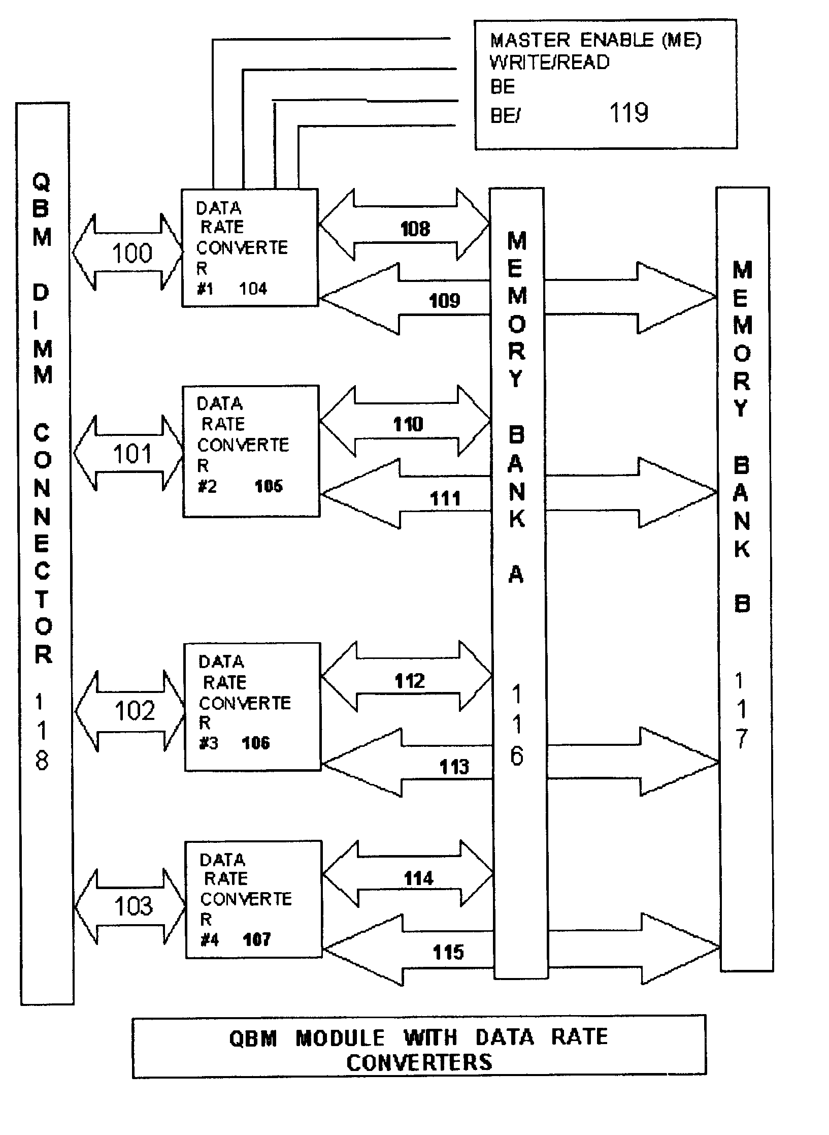
15DETAILED DESCRIPTIONThe current invention is a high speed Data Rate Converting and Switching Circuit for use in high speed memory systems in modern computers. The present invention is used in conjunction with a high-speed computer memory system, such as that disclosed in U.S. Pat. No. 6,446,158, issued on Sep. 3, 2002 to Chris Karabatsos, the inventor of the current invention. Said prior application Ser. No. 6,446,158 is incorporated herein by reference, in its entirety, for the purpose of describing the application and utility of the present invention, and for describing further the interface between the present invention and external devices not part of the present invention.

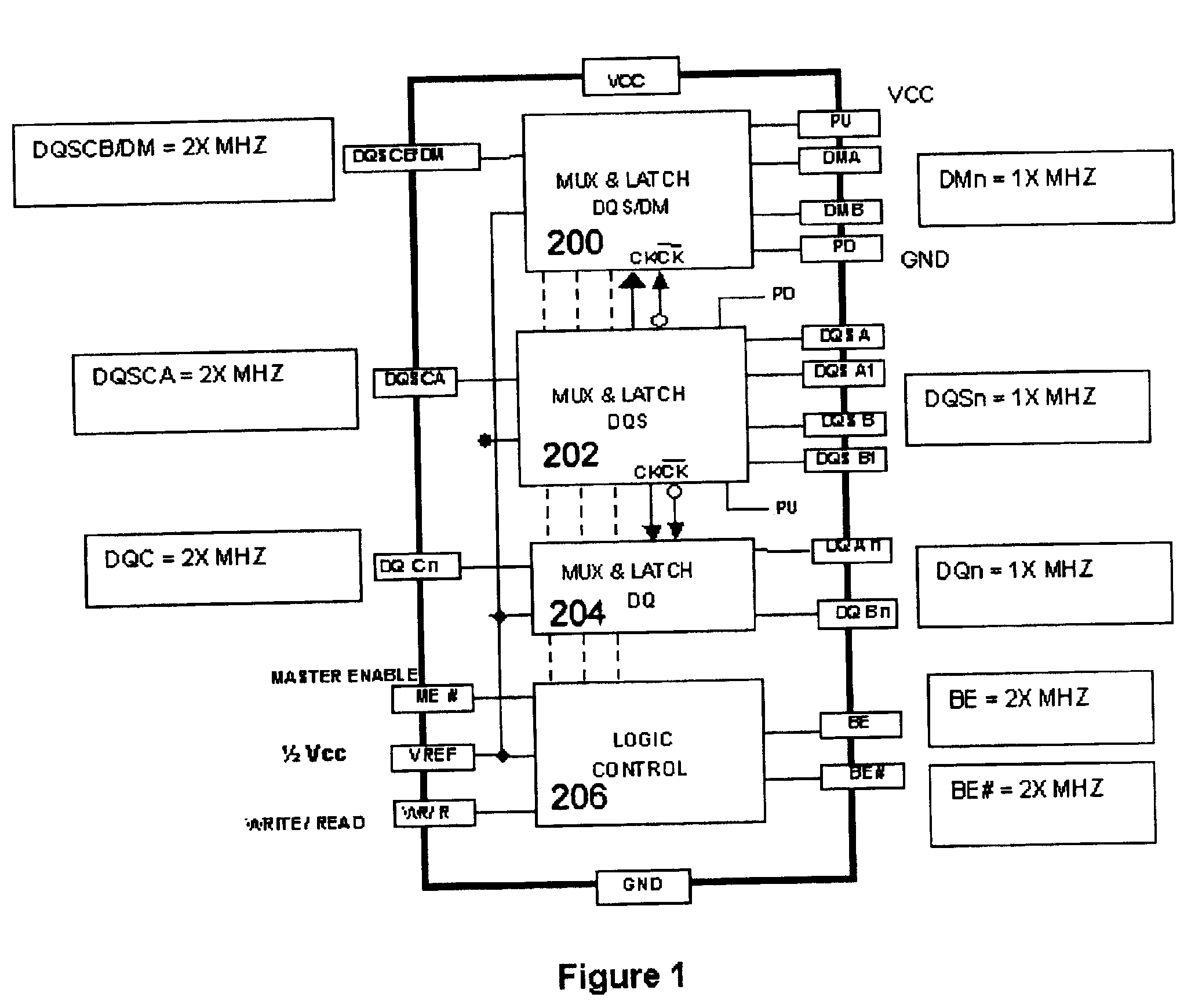
SIGNAL DEFINITIONS In the following description, the signals will be identified as follows. Unless otherwise indicated, the identities of the signals and the ports on which the signals appear are used interchangeably.

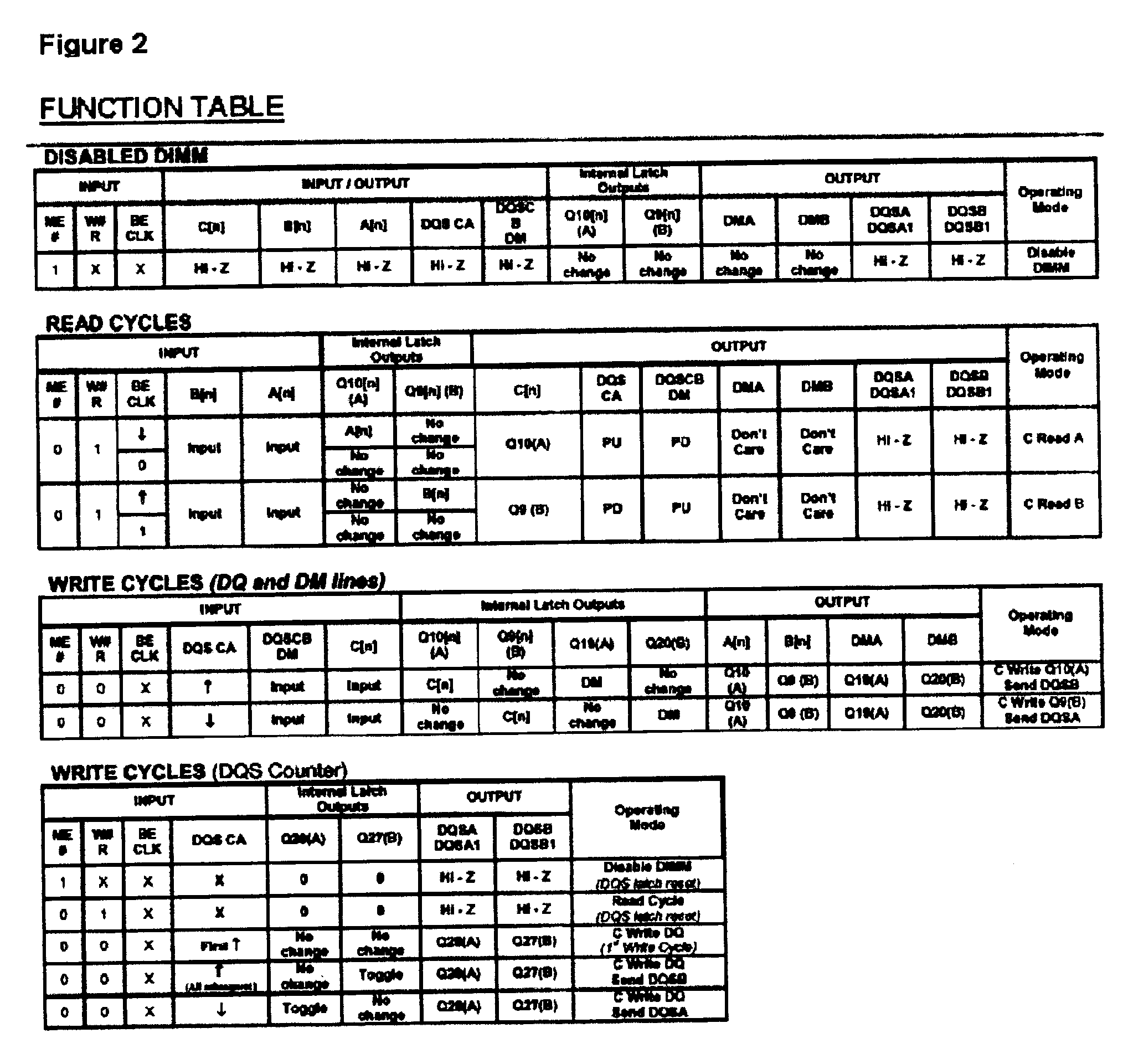
ME (Master Enable) The ME signal has as primary function to enable or disable the device so ...


PUM


Abstract

A high speed bidirectional data rate conversion circuit converts 1× data rate signals from attached devices on port A and port B to 2× data rate signals on bus C and further converts 2× high speed data rate signals on bus C to 1× data rate signals on ports A and B for memory devices attached to ports A and B. The usage of pass gate switches and combination of latches and counters is used to permit proper synchronization of the data signals, and to further generate strobe signals at both system bus and memory bus sides, and to further generate data mask signals for writing to the memory bus side of the circuit. The collection of such switching elements and latches are provided on a single silicon chip which includes of the functions of the invention.

Description

BACKGROUND OF INVENTIONThis application claims priority based on provisional patent No. 60 / 397,491 filed on Jul. 22, 2002 by the applicant of the present invention.The computer industry, with the advances of silicon technology, is constantly faced with the complexities of high speed Data Buses. The high speed of microprocessor CPU requires high speed of data bus between the memory subsystem and the front end CPU data bus. However, speed without density of memory is an unbalanced combination. Modern computer systems require increasingly large RAM arrays, and these arrays are packaged in modules of approximately the same size as used in previous, lower capacity memories. Thus, the density of the memory modules, in bits or bytes per square inch of circuit board, is constantly increasing.The CPU by itself cannot increase computer performance without a high speed memory sub-system and it does not perform at the speed it was designed for. When memory access is substantially slower than CP...

Claims


Application Information

Patent Timeline
IPC IPC(8): G06F12/00
CPCG06F13/4234G06F13/405
Inventor KARABATSOS, CHRIS
Owner URENSCHI ASSETAB LIABILITY
Why Eureka
Try Eureka