Optical wiring device

a wiring device and optical technology, applied in the field of optical wiring devices, can solve the problems of signal delay, heat generation and electromagnetic radiation emission noise (emi) due to electric wiring, and the solution of those problems is difficult, and the limitations of electric wiring will be a serious problem, so as to achieve the effect of reducing cost and being adaptabl

Inactive Publication Date: 2005-02-15
CANON KK
View PDF18 Cites 51 Cited by
  • Summary
  • Abstract
  • Description
  • Claims
  • Application Information

AI Technical Summary

Benefits of technology

It is an object of the present invention to provide an optical wiring device which includes a built-in E / O and / or O / E converting portion, an electric connecting portion and an optical transmitting waveguide, which is readily adaptable to optical interconnection, and whose cost can be reduced, and so forth.
Furthermore, the present invention is directed to an electronic apparatus, wherein a computer body with a device, such as a central processing unit (CPU), mounted therein and a display with an input / output (I / O) port are connected to each other by the above optical wiring device, and / or wherein the computer body and a network, such as a local area network (LAN), are connected to each other by the above optical wiring device. Also in this structure, the same technical advantages as above can be obtained.

Problems solved by technology

At the same time, problems of signal delay, heat generation and electromagnetic radiation emission noise (EMI) due to the electric wiring occur in connections between boards in electronic equipment, between a board and a built-in device, and between electronic equipment.
Solutions of those problems are, however, difficult.
It is hence apparent that limitations in the electric wiring will be a serious problem in the near future.
The range of its use is, however, restricted since costs of its interface IC and cable, such as a twinax cable, are high.
Further, in its high-speed transmission at about 1 Gbps, impedance matching is required, and its transmission distance is limited to about 10 m.
However, when its total rate exceeds 1 Gbps, problems occur due to the number of pins, connector reliability, space, skew (delay between channels), and the cost and weight of cables.
Furthermore, in either case, the problem of EMI is serious in the electric wiring, and its seriousness increases as the transmission speed becomes faster.
There is, however, the problem that precise implementation of optical connector and optical device is required to reduce optical losses, and hence, its cost increases and the system is difficult to put into practice.
Further, when a large number of channels and optical connecting portions are needed to achieve a large-capacity transmission, problems of yield and space occur, and hence, its use in place of the electric wiring is limited.
Furthermore, the system is not reliable for frequent loading and unloading, and ordinary handling is not easy.
Therefore, the system is not suitable for use in electronic equipment intended for general consumers.
In the system of FIG. 2, however, yield is likely to decrease and there is a limitation to a compact size, because a plurality of high-performance devices (i.e., optical modulators 1107) are arranged on the optical MCM 1101.
Thus, the size of the structure increases, and bending handling is restricted.

Method used


Image

  • Optical wiring device
  • Optical wiring device
  • Optical wiring device

Examples


first embodiment

(First Embodiment)

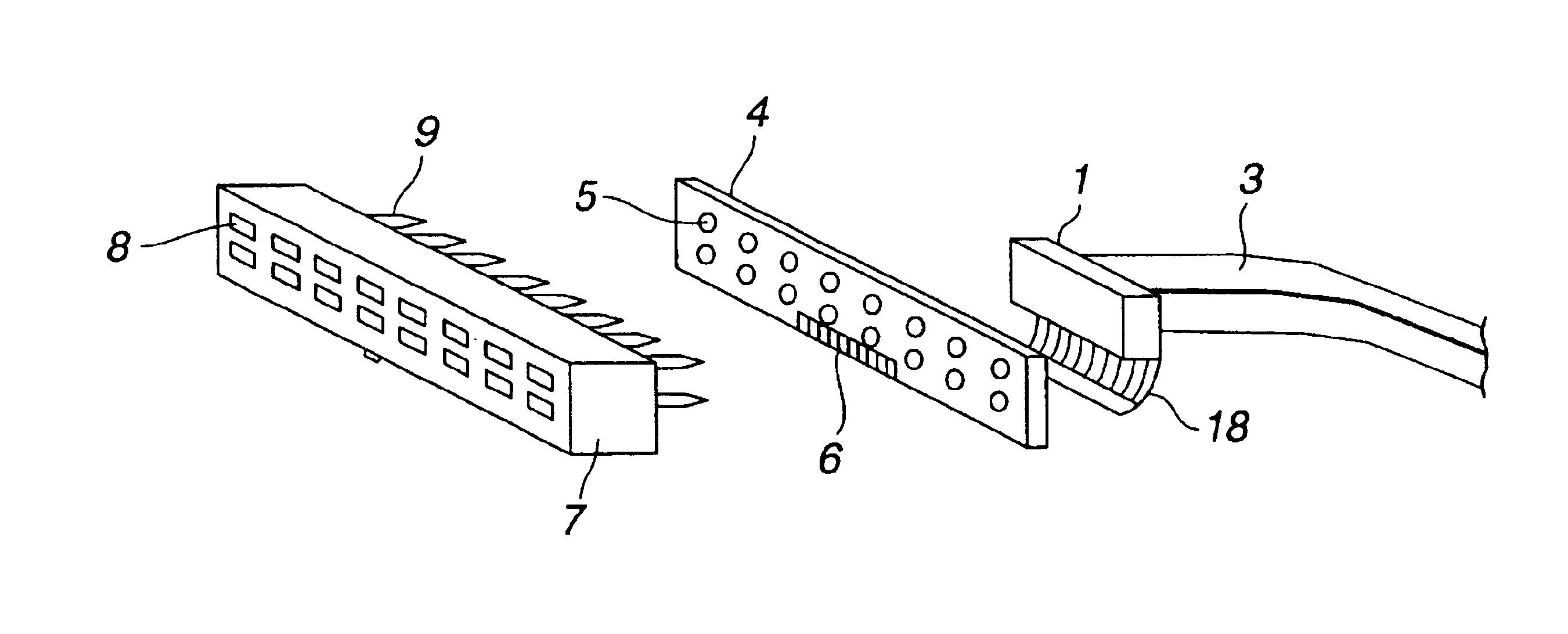
FIG. 3A illustrates structures of electric and optical connecting portions of a first embodiment of the present invention directed to an optical wiring device. In the optical wiring device of FIG. 3A, a connecting portion 7 for electric connection is provided, and the electric connecting portion 7 includes a recessed electric coupler of two-dimensionally arranged recesses 8 and two-dimensionally arranged pins 9 for electrically connecting the corresponding recesses 8 to rear-stage electric wires. The connecting portion 7 is composed of a conventional resin, for example. There are sixteen (16=2×8) pins 9 in the structure of FIG. 3A, but the number thereof is not limited to this configuration. The recesses 8 may be replaced by protruding pins.

At the rear of the connecting portion 7, there is provided a plate 4 including two-dimensionally arranged holes 5, serially arranged electrode pads 6, and a wiring pattern (not shown) for electrically connecting each hole 5 to e...

second embodiment

(Second Embodiment)

The first embodiment is directed to an optical wiring device which is principally used for parallel wiring. In this case, as the number of pins increases, the area occupied by the connecting portion and the volume of the multi-core waveguide also increase.

In the light of such a disadvantage, a second embodiment is directed to an optical wiring device in which parallel-to-serial conversion is partially conducted to decrease the number of pins and the features of the surface optical device (i.e., high-speed transmission) are utilized. In the second embodiment, a connecting pin 91 is fixed to a base plate 90 as illustrated in FIG. 11A. The protruding pin 91 is connected to a board 100 through a recessed receptacle 98 mounted to the board 100 as illustrated in FIG. 11B, or directly bonded to the board 100 with a solder 103. At the rear of the base plate 90, there is provided a bare chip 92 of a Si-IC in which a parallel-to-serial conversion IC and a laser-driving IC a...

third embodiment

(Third Embodiment)

In the first and second embodiments, the multi-core waveguide fabricated by the surface process is used as the optical cable. However, when the length of the wiring between apparatuses, for example, is over 1 m, the structure using an optical fiber is more advantageous in a total cost. Therefore, in a third embodiment, an optical wiring connector is constructed by using a fiber array.

FIG. 14 illustrates the structure of the third embodiment. As illustrated in FIG. 14, pins 121 for electric connection are arranged on an electric connecting portion 120, and a Si-IC 122 is implemented on the connecting portion 120 in a flip-chip manner such that the Si-IC 122 is connected to the pins 121.

In the Si-IC 122, similarly to the second embodiment, driving ICs for the surface emitting laser and the surface light receiving device are integrated. The Si-IC 122 has a region for the implementation of optical devices 123 and electrode pads, similarly to the second embodiment. The ...


PUM


Abstract

An optical wiring device includes an electric connecting portion, an optical transmission unit for transmitting an optical signal, and an optical device for conducting an optoelectric conversion. The optical device is provided between the electric connecting portion and the optical transmission unit. The optical device includes at least one of a surface light emitting device, which is modulated by an electric signal supplied through the electric connecting portion, and a surface light receiving device, which converts an optical signal transmitted through the optical transmission unit to an electric signal.

Description

BACKGROUND OF THE INVENTION1. Field of the InventionThis invention relates to an optical wiring device, such as an optical connector and a waveguide cable, for optically connecting electronic equipment, boards in electronic equipment, or apparatuses to each other, its driving method, and so forth.2. Related Background ArtIn recent years, the speed of computers, information processing, and computer environment, including displays and printers, has been increasing. At the same time, problems of signal delay, heat generation and electromagnetic radiation emission noise (EMI) due to the electric wiring occur in connections between boards in electronic equipment, between a board and a built-in device, and between electronic equipment. Solutions of those problems are, however, difficult. It is hence apparent that limitations in the electric wiring will be a serious problem in the near future.Between apparatuses, a system has been developed in which fast transmission by giga-bit Ethernet a...

Claims


Application Information

Patent Timeline
Patent Type & Authority Patents(United States)
IPC IPC(8): G02B6/42G02B6/02G06F1/18G02B6/122G02B6/43G06F3/00H01L31/0232H01L31/12H01R13/46H01S5/022H01S5/18H04B10/25H04B10/80
CPCG02B6/1221G02B6/4201G02B6/4249G02B6/4292G02B6/43G02B6/02033H01R9/091G02B6/4246
Inventor OUCHI, TOSHIHIKO
Owner CANON KK
Why Eureka
Try Eureka