Liquid crystal display (LCD) devices having redundant patterns

a liquid crystal display and redundant technology, applied in non-linear optics, instruments, optics, etc., can solve the problems of light leakage, easy defect of liquid crystal display transistors by electrostatic discharge, complicated methods, etc., and achieve the effect of reducing light leakag

Inactive Publication Date: 2005-02-15
SAMSUNG ELECTRONICS CO LTD
View PDF13 Cites 44 Cited by
  • Summary
  • Abstract
  • Description
  • Claims
  • Application Information

AI Technical Summary

Benefits of technology

In view of the above, it is an object of the present invention to reduce the light leakage of IPS mode liquid crystal displays.
It is another object of the present invention to prevent thin film transistors from being destroyed by the electrostatic discharge.
It is another object of the present invention to simplify the manufacturing process of IPS mode liquid crystal displays.
It is another object of the present invention to decrease the opening of wires.
It is another object of the present invention to increase the reliability of the contacts between pads and drivers
A passivation layer which is thick relative to the pixel wire may have relatively flat surface since the pixel wire is relatively thin. The flat surface may give rise to uniform rubbing and thus the light leakage may be reduced.

Problems solved by technology

However, since the two kinds of electrodes are made of different layers and have different thickness, the surface of the alignment layer may not be flat, and this causes non-uniform rubbing which may result in light leakage.
Moreover, the liquid crystal display of Kondo et al., in particular, transistors of the liquid crystal display are easily defected by the electrostatic discharge because the two electrodes are formed together on a single substrate.
However, this method is complicated.

Method used


Image

  • Liquid crystal display (LCD) devices having redundant patterns
  • Liquid crystal display (LCD) devices having redundant patterns
  • Liquid crystal display (LCD) devices having redundant patterns

Examples


first embodiment

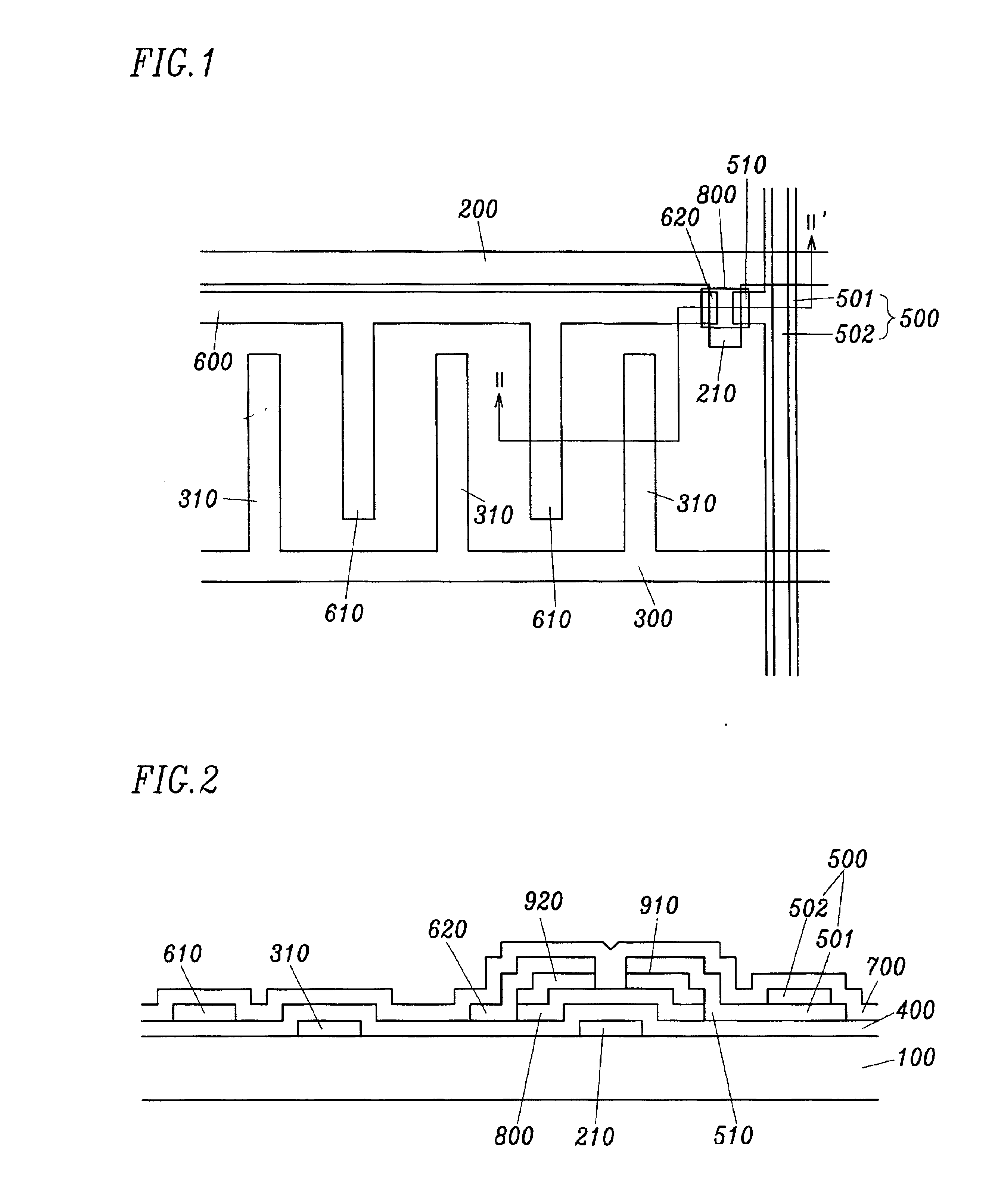
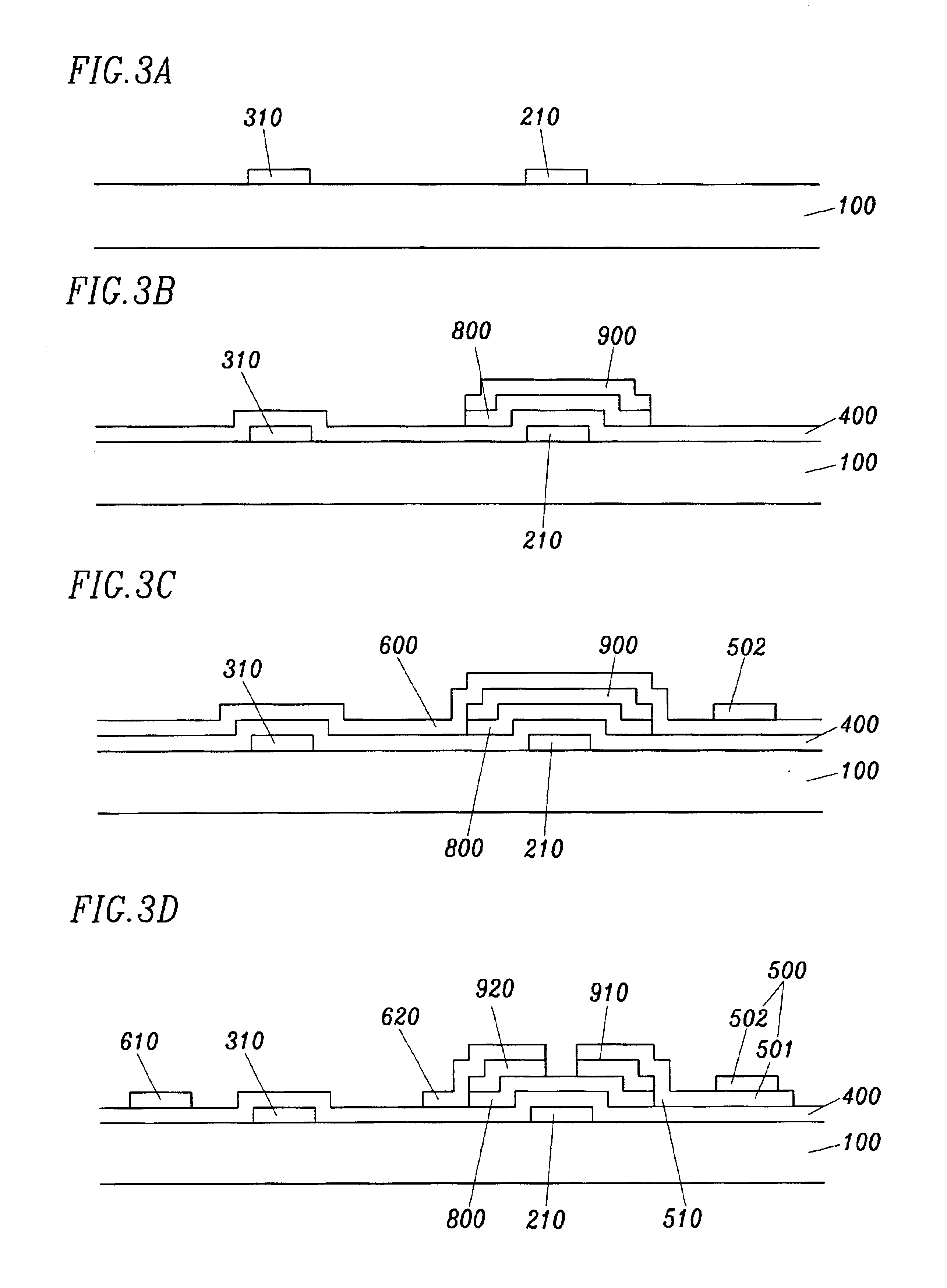
First, the structure of a panel for a liquid crystal display according to the present invention will be described. FIG. 1 is a layout view of a panel, and FIG. 2 is a cross-sectional view of the panel illustrated in FIG. 1 taken along the line II-II′.

A gate wire including a transverse gate line 200 and a gate electrode 210 which is a branch of the gate line 200 is formed on a substrate 100. A common signal wire including a common signal line 300 parallel to the gate line 200 and a plurality of linear common electrodes 310 connected to the common signal line 300 is also formed on the substrate 100. The common electrodes 310 extend toward the gate line 200, and they are spaced apart from each other and parallel to each other.

A gate insulating layer 400 is formed over the gate wire 200 and 210 and the common signal wire 300 and 310.

A channel layer 800 and an ohmic contact layer 910 and 920 are sequentially formed on a portion of the gate insulating layer 400 over the gate electrode 210...

second embodiment

Now, the present invention is described, where a pixel wire and a data wire have small thickness and a relatively thick redundant data pattern connected to the data wire is provided on a passivation layer.

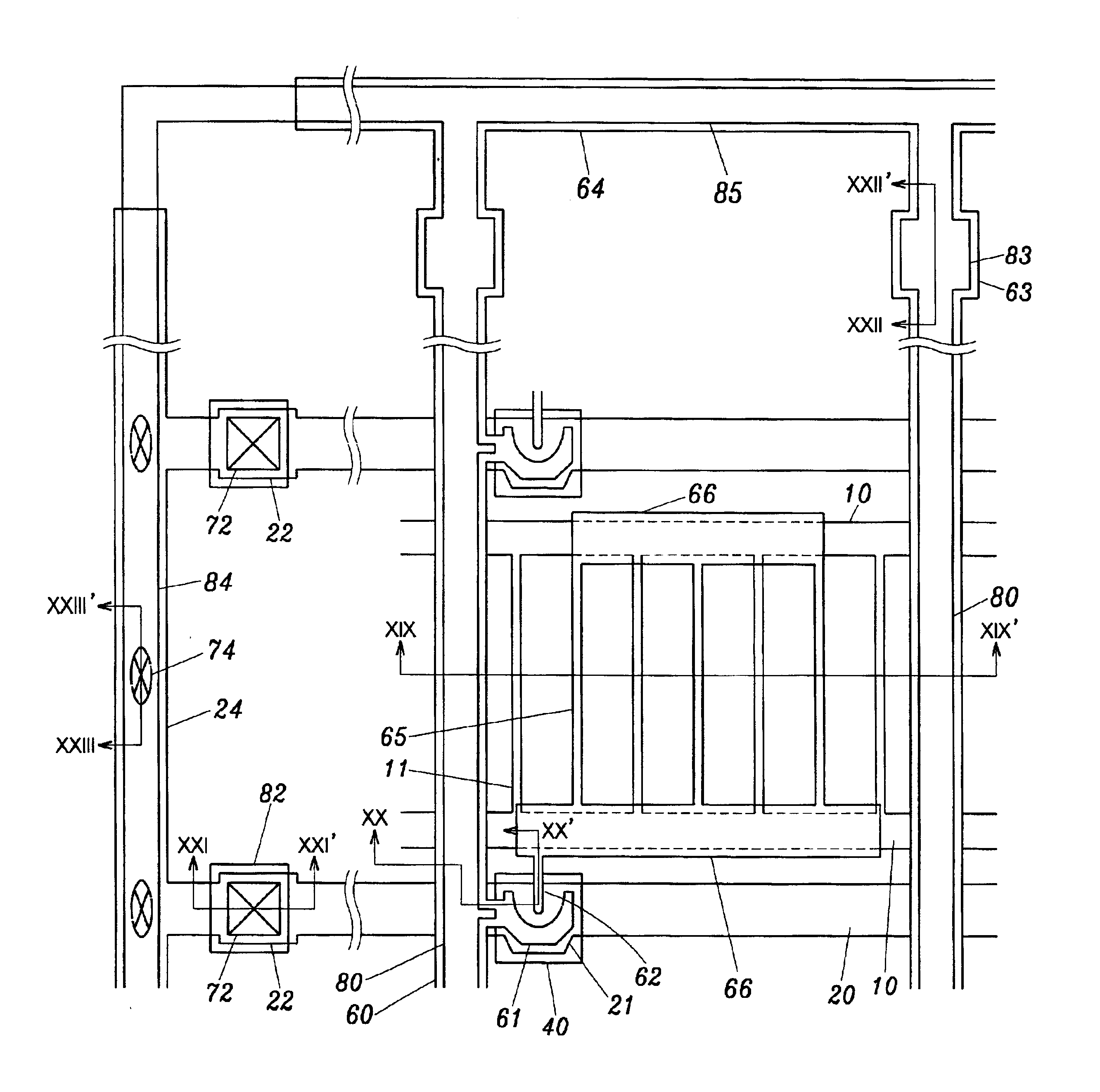
First, the structure of the panel for a liquid crystal display according to the second embodiment will be described. FIG. 4 is a schematic diagram of the LCD panel according to the second embodiment.

As shown in FIG. 4, a plurality of gate lines 20 extending in a transverse direction are formed on a substrate 100, and a plurality of common signal lines 10 on the substrate 110 are arranged parallel to the gate lines 20. A plurality of gate pads 22, which are connected to external gate drivers (not shown), are formed to be connected to the ends of the gate lines 20. A gate line connector 24 is formed in a longitudinal direction and connected to the gate pads 22 via its branches. A plurality of data lines 60 extending in the longitudinal direction intersect and are insulated from the g...


PUM

PropertyMeasurementUnit
conductiveaaaaaaaaaa
thicknessaaaaaaaaaa
electric fieldsaaaaaaaaaa

Abstract

A gate wire including a gate line, a gate electrode, a gate pad and a gate line connector and a common signal wire are formed on a substrate, and a gate insulating layer is formed over the gate wire and the common signal wire. A semiconductor layer and an ohmic contact layer are sequentially formed on the gate insulating layer, a data wire including a source and a drain electrode, a data line, a data pad and a data line connector and a pixel electrode are formed thereon. The thickness of the data wire and the pixel electrode is equal to or less than 500 Å. A passivation layer is formed on the data wire and the pixel electrode, a redundant data wire is formed thereon, and a redundant gate pad and a redundant gate line connector are formed. The redundant data wire is electrically connected to the data wire through the contact holes in the passivation layer, and the redundant gate pad and the redundant gate line connector are electrically connected to the gate pad and the gate line connector respectively through the contact holes in the passivation layer and the gate insulating layer. The redundant gate line connector and the redundant data line connector are connected to each other to short the gate and the data wires. After an alignment layer is formed and rubbed, the edge of the panel is cut away to remove the gate line connector and the data line connector.

Description

BACKGROUND OF THE INVENTIONa. Field of the InventionThe present invention relates to liquid crystal displays and manufacturing methods thereof, more specifically to liquid crystal displays having electrode arrays for applying electric fields parallel to substrates and thin film transistors as switching elements and manufacturing methods thereof.b. Description of the Related ArtA liquid crystal display (LCD) having an electrode array for generating an electric field which is parallel to substrates (IPS mode; in-plane switching mode) is disclosed in U.S. Pat. No. 5,598,285 of Kondo et al.The IPS mode LCD of Kondo et al. has two substrates opposite each other and a liquid crystal layer therebetween. Two kinds of electrodes for generating electric field, common electrodes and pixel electrodes are formed on one of the substrates. An alignment layer is coated on the electrodes.However, since the two kinds of electrodes are made of different layers and have different thickness, the surface...

Claims


Application Information

Patent Timeline
Patent Type & Authority Patents(United States)
IPC IPC(8): G02F1/13G02F1/1362
CPCG02F1/136204
Inventor SONG, JUN-HOLEE, KYEONG-NAM
Owner SAMSUNG ELECTRONICS CO LTD
Why Eureka
Try Eureka