
System and method for programming cells in non-volatile integrated memory devices

a technology of integrated memory and programming system, which is applied in the field of non-volatile integrated memory devices, can solve the problems of increasing the power consumption of programming the large number of memory cells in a sector, further limitations on the ability to program large numbers of memory cells in parallel, etc., and achieves the effect of quick and efficient programming of hard-to-program storage elements

Inactive Publication Date: 2005-02-15
SANDISK TECH LLC
View PDF13 Cites 89 Cited by
  • Summary
  • Abstract
  • Description
  • Claims
  • Application Information

AI Technical Summary

Benefits of technology

It is an object of the present invention to provide a system and method for quickly and efficiently programming hard-to-program storage elements in non-volatile integrated memory devices. According to a principle aspect of the present invention, a number of storage elements are simultaneously subjected to a programming process with the current flowing through the storage elements limited to a first level. As a portion of these storage elements reach a prescribed state, they are removed from the set of cells being programmed and the current limit on the elements that continue to be programmed is raised. Although this results in the amount of current flowing per element increasing, since the number elements in which it flows is decreased, the cumulative current flowing can be maintained at a low level while still applying greater current to hard-to-program storage elements.
In an embodiment employing a Flash EEPROM memory, a circuit is provided for quickly and efficiently programming memory cells in a programmable memory device that reduces the instantaneous and average programming current with little or no reduction in programming speed. In general, the method involves applying a set of voltage waveforms to the various gates, and drains of the memory cells that are targeted for programming while limiting drain to source current (IDS) through each of the selected memory cells to a predetermined level by raising the source voltage (source de-biasing) and applying at least one programming pulse to the memory cells. For the cells that need further programming, the IDS limited is raised and further programming pulses are applied.
In yet another embodiment, the internal memory chip's peripheral circuits are configured to control the current limiter to provide the higher current to each hard-to-program memory cell after a predetermined number of the selected memory cells have been programmed. In a further embodiment, the various aspect of the invention can be applied to a soft programming process, which is other wise known as erase recovery. There may exist defective memory cells that have already been mapped out of the logical sector and are hard to soft program under source debasing conditions. These memory cells may be soft programmed with a grounded source, so as to eliminate parasitic current paths that introduce read errors when a deselected over erased memory cell (that is intended to be off) actually conducts.

Problems solved by technology

However, as a large number of storage units are generally programmed in parallel, with the trend being towards even greater numbers, this results in high current levels, both on average and instantaneously, that are at odds with the trend to lower power devices.
Power consumed in programming the large number of memory cells in a sector has become a significant problem in conventional flash memories.
It is particularly a problem for portable devices that rely on batteries and generally have an on-chip voltage supply or charge pump with a limited power capacity.
Thus, the increasing number memory cells and the shrinking battery sizes in portable devices have introduced further limitations on the ability to program large numbers memory cells in parallel.

Method used


Image

  • System and method for programming cells in non-volatile integrated memory devices
  • System and method for programming cells in non-volatile integrated memory devices
  • System and method for programming cells in non-volatile integrated memory devices

Examples


Embodiment Construction

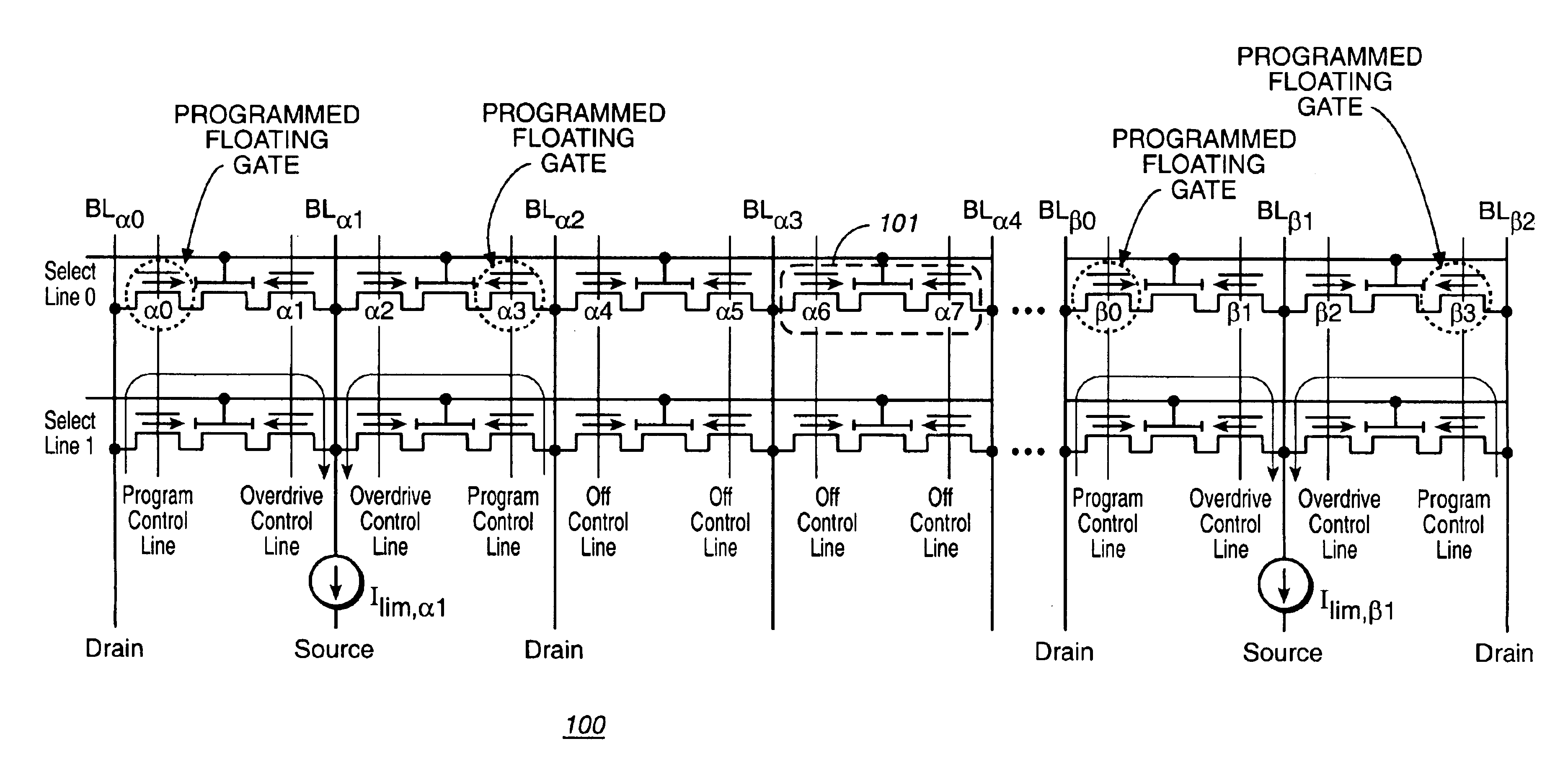
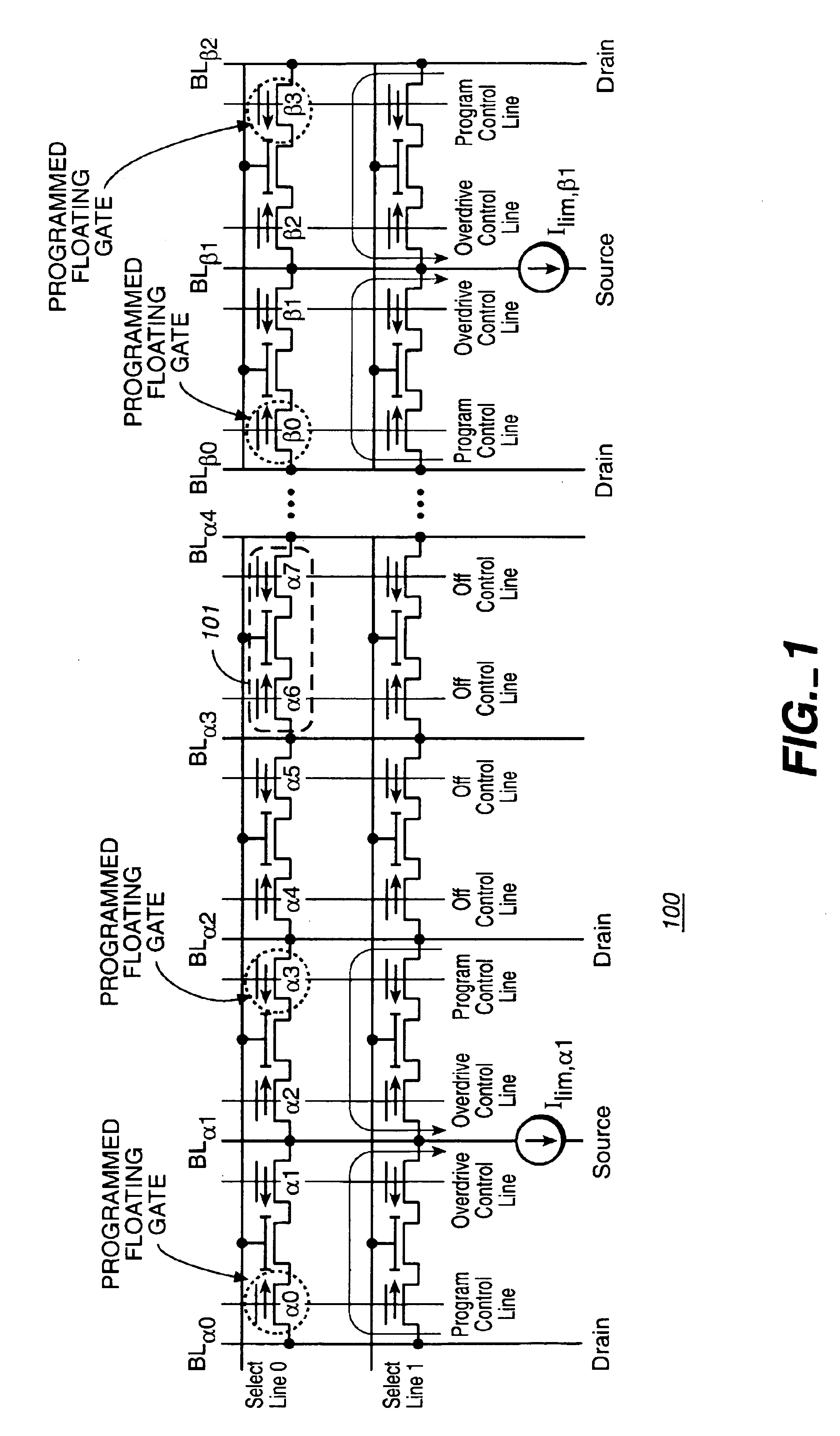
FIG. 1 shows an exemplary embodiment of a portion of a non-volatile memory array 100. In this particular embodiment, each storage unit is a dual floating gate EEPROM unit that is programmed by source side injection. For example, an individual storage unit 101 has floating gate transistors α6 and α7 on either side of a select gate transistor connected between bit lines BLα3 and BLα4 in a virtual ground arrangement. Two rows, connected to Select Lines 0 and 1, and two blocks, the α and β areas, of array 100 are shown in FIG. 1, with the actual array generally being much larger. The individual floating gate transistors can each store two or more data states.

The various aspects of the present invention are not particular to the specific type of array shown in FIG. 1, but this structure will often be used as an exemplary embodiment since it can readily illustrate many of the aspects of the present invention. As described in the Background section, current non-volatile memory systems ofte...


PUM


Abstract

A system and method for quickly and efficiently programming hard-to-program storage elements in non-volatile integrated memory devices is presented. A number of storage elements are simultaneously subjected to a programming process with the current flowing through the storage elements limited to a first level. As a portion of these storage elements reach a prescribed state, they are removed from the set of cells being programmed and the current limit on the elements that continue to be programmed is raised. The current level in these hard-to-program cells can be raised to a second, higher limit or unregulated.

Description

TECHNICAL FIELDThe present invention relates generally to non-volatile integrated memory devices and, more particularly, to a system and method for controlling current levels during the programming of non-volatile integrated memory devices.BACKGROUNDIn many non-volatile computer memories, the ability to store data is often related to the amount of current that flows through a particular storage unit during the programming process. One particular example of a non-volatile memory is a Flash or EEPROM memory where the state of a storage unit within the memory is dependent on the amount of charge stored on a floating gate. In general terms, the greater the current that flows through a given unit, the quicker it can be programmed, the wider range of levels to which it can be programmed, or both. However, as a large number of storage units are generally programmed in parallel, with the trend being towards even greater numbers, this results in high current levels, both on average and insta...

Claims


Application Information

Patent Timeline
IPC IPC(8): G11C11/56G11C16/04G11C16/10G11C16/34
CPCG11C16/0458G11C16/3454G11C16/10G11C16/02
Inventor MOKHLESI, NIMAPASTERNAK, JOHN H.
Owner SANDISK TECH LLC
Features
  • Generate Ideas
  • Intellectual Property
  • Life Sciences
  • Materials
  • Tech Scout
  • Unparalleled Data Quality
  • Higher Quality Content
  • 60% Fewer Hallucinations
Learn More