Solid-state image pickup apparatus and control method thereof

a technology of solid-state image and pickup apparatus, which is applied in the direction of radiation control devices, distance measurement, instruments, etc., can solve the problems of high chip power consumption, difficult to reduce the size of the sensor and increase the number of pixels of the sensor, and unsuitable for consumer applications, so as to reduce the size of the apparatus, simplify the configuration of the pixels, and enhance the function of obtaining

Inactive Publication Date: 2005-02-22
SONY CORP
View PDF4 Cites 37 Cited by
  • Summary
  • Abstract
  • Description
  • Claims
  • Application Information

AI Technical Summary

Benefits of technology

Therefore, circuit elements required for each of the signal processing operations are arranged together outside pixels, so that a configuration within each of the pixels can be simplified and minimized. Also, it is possible to enhance the function of obtaining a normal actual image and the com

Problems solved by technology

However, since the image sensor as described above retains the computational circuit in each of the pixels, the pixels have a large size, and therefore it is difficult to reduce size of the sensor and increase the number of pixels of the sensor.
In addition, the large circuit scale results in a high power consumption by the chip, specifically a power consumption of 1 W or more according to the first conventional literature, for example.
Such an

Method used


Image

  • Solid-state image pickup apparatus and control method thereof
  • Solid-state image pickup apparatus and control method thereof
  • Solid-state image pickup apparatus and control method thereof

Examples


first embodiment

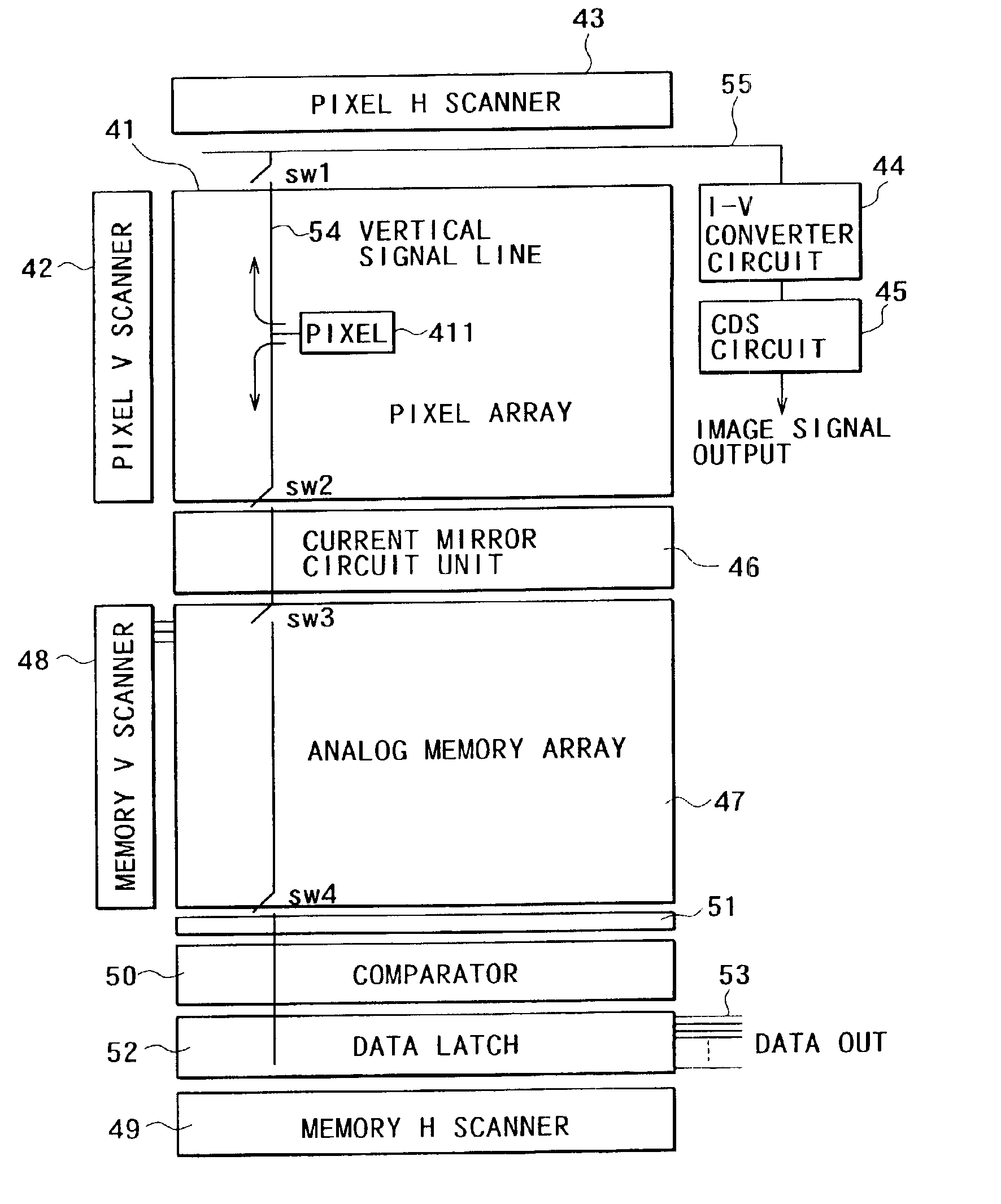
FIG. 1 is a plan view of a general configuration of an image sensor according to the present invention.

As shown in FIG. 1, the image sensor includes a pixel array unit 41, a pixel V scanner unit 42, a pixel H scanner unit 43, an I-V converter circuit unit 44, a CDS circuit unit 45, a current mirror circuit unit 46, an analog memory array unit 47, a memory V scanner unit 48, a memory H scanner unit 49, a comparator unit 50, a bias circuit unit 51, a data latch unit 52, an output data bus unit 53 and the like.

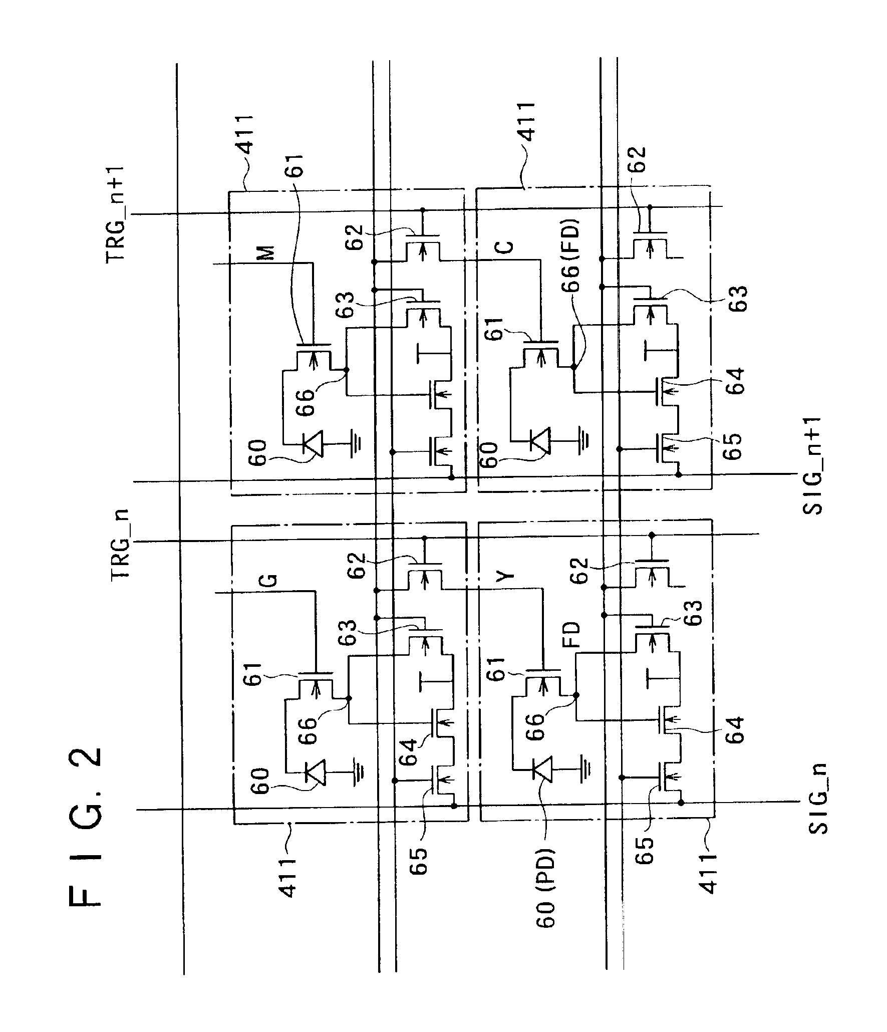
The pixel array unit 41 is formed by arranging a plurality of pixels 411 for detecting light in a two-dimensional matrix form in a row direction and a column direction. A signal sent out from each of the pixels 411 is transmitted by a signal line (vertical signal line) 54 extending in a vertical direction.

The pixel V scanner unit 42 and the pixel H scanner unit 43 scan an interior of the pixel array unit 41 in the vertical direction and the horizontal direction to thereby select ...

second embodiment

the present invention will next be described.

The solid-state image pickup apparatus according to the first embodiment as described above realizes functions of normal color image output and three-dimensional range measurement based on a light-section method. The method of three-dimensional range measurement can be realized by the conventional configuration described with reference to FIG. 6A.

Specifically, a light source emitting a stripe of light and a scanning mirror are disposed in the vicinity of a sensor (light receiving unit). A subject is irradiated with the stripe of light via the mirror while scanning the scanning mirror. Range information for each point of the subject can be obtained from a relation between timing in which each pixel of the sensor receives the stripe of light reflected from the subject and a scan angle of the mirror on principles of triangulation.

In this case, however, many parts such as the light source, an optical device for generating the stripe of light,...

third embodiment

the present invention will next be described.

FIGS. 11A and 11B are diagrams of assistance in explaining two configuration examples of a three-dimensional range measurement system according to the third embodiment of the present invention.

The system for the light-section method in this example uses a laser hologram 100 in a light projecting unit for providing a stripe of light.

The laser hologram is commercialized and used as an AF light source of a digital still camera, for example. As shown in FIGS. 11A and 11B, the laser hologram is disposed in a path of light emitted from a laser light source 101, and controls laser light into a stripe of light and supplies the stripe of light to an object 102.

Light reflected from the object 102 is passed through a lens 111 and then shot by a sensor 110 as described in the first embodiment, whereby three-dimensional range measurement is performed.

It is to be noted that while in this example, the same mirror scanner (scanner mirror) 103 as in the e...


PUM


Abstract

An arithmetic circuit, which is retained by each pixel in a conventional image sensor, is shared by each column. Signal processing circuits of different configurations are provided on signal transmission paths in an upward direction and a downward direction of a vertical signal line for extracting an image signal from each pixel, whereby image output processing and arithmetic processing are performed completely separately by the different circuit blocks. Thus, image quality of an actual image is improved and optimum design for arithmetic processing is made possible. Specifically, an I-V converter circuit unit, a CDS circuit unit and the like are provided on the image output side. A current mirror circuit unit, an analog memory array unit, a comparator unit, a bias circuit unit, a data latch unit, an output data bus unit and the like are provided on the arithmetic processing side.

Description

BACKGROUND OF THE INVENTIONThe present invention relates to a solid-state image pickup apparatus and a control method thereof having a function of obtaining a normal image signal and additionally a computational function for executing various applications.Recently, solid-state image pickup apparatus have been proposed which image sensors have a function of performing various operations on image information and thereby realize an increase in the speed of image processing and the like.As one of such image sensors, a sensor having a function of obtaining a normal actual image, a function of three-dimensional range calculation, and a function of detecting a moving object has been proposed (see ISSCC / 2001 / SESSION6 / CMOS IMAGE SENSORS WITH EMBEDDED PROCESSORS / 6.4 (2001IEEE International Solid-State Circuits Conference) and Japanese Patent Application No. 2000-107723, for example; in the following description, the former will be described as first conventional literature, and the latter wil...

Claims


Application Information

Patent Timeline
IPC IPC(8): H04N3/15H04N5/335G01C3/06H01L27/146H04N5/341H04N5/369H04N5/374H04N5/378H04N9/07
CPCH04N5/335H04N3/155H01L27/14609H04N25/00H04N25/767H04N25/76
Inventor SUGIYAMA, TOSHINOBUYOSHIMURA, SHINICHISUZUKI, RYOJIHOSHINO, KAZUHIRO
Owner SONY CORP
Why Eureka
Try Eureka