I/O circuit using low voltage transistors which can tolerate high voltages even when power supplies are powered off

a low-voltage transistor and high-voltage technology, applied in logic circuit coupling/interface arrangement, pulse technique, instruments, etc., can solve the problems of i/o circuit pad operating voltage being insufficient, ic may fail, and proportionally decreasing the maximum operating voltage that the semiconductor devices within the ic can withstand. to prevent device stress

Inactive Publication Date: 2005-02-22
AVAGO TECH INT SALES PTE LTD
View PDF72 Cites 28 Cited by
  • Summary
  • Abstract
  • Description
  • Claims
  • Application Information

AI Technical Summary

Problems solved by technology

Unfortunately, reducing the IC feature sizes may proportionally decrease the maximum operating voltage that the semiconductor devices within the IC can withstand.
In such a case the maximum operating voltage of the I / O circuit pad is insufficient to drive the external components which have a higher voltage requirement, such as 5 volts.
Furthermore, if the IC is interfaced with a greater than the maximum operating voltage, the IC may fail.
However, this voltage robustness is commonly accompanied by a decrease in the performance of the IC, because the thick gate-oxide layer reduces the overall gain of the devices which comprise the IC.
The resulting hybrid process may significantly increase the manufacturing costs of the IC.
Such a level-shift chip can be a waste of much needed space on a crowded printed circuit board and may degrade performance.
When the I / O power supply varies, circuits may have higher stress on the gate-oxides of the devices in the I / O circuit, such stresses may not be desirable in many process technologies.

Method used


Image

  • I/O circuit using low voltage transistors which can tolerate high voltages even when power supplies are powered off
  • I/O circuit using low voltage transistors which can tolerate high voltages even when power supplies are powered off
  • I/O circuit using low voltage transistors which can tolerate high voltages even when power supplies are powered off

Examples


Embodiment Construction

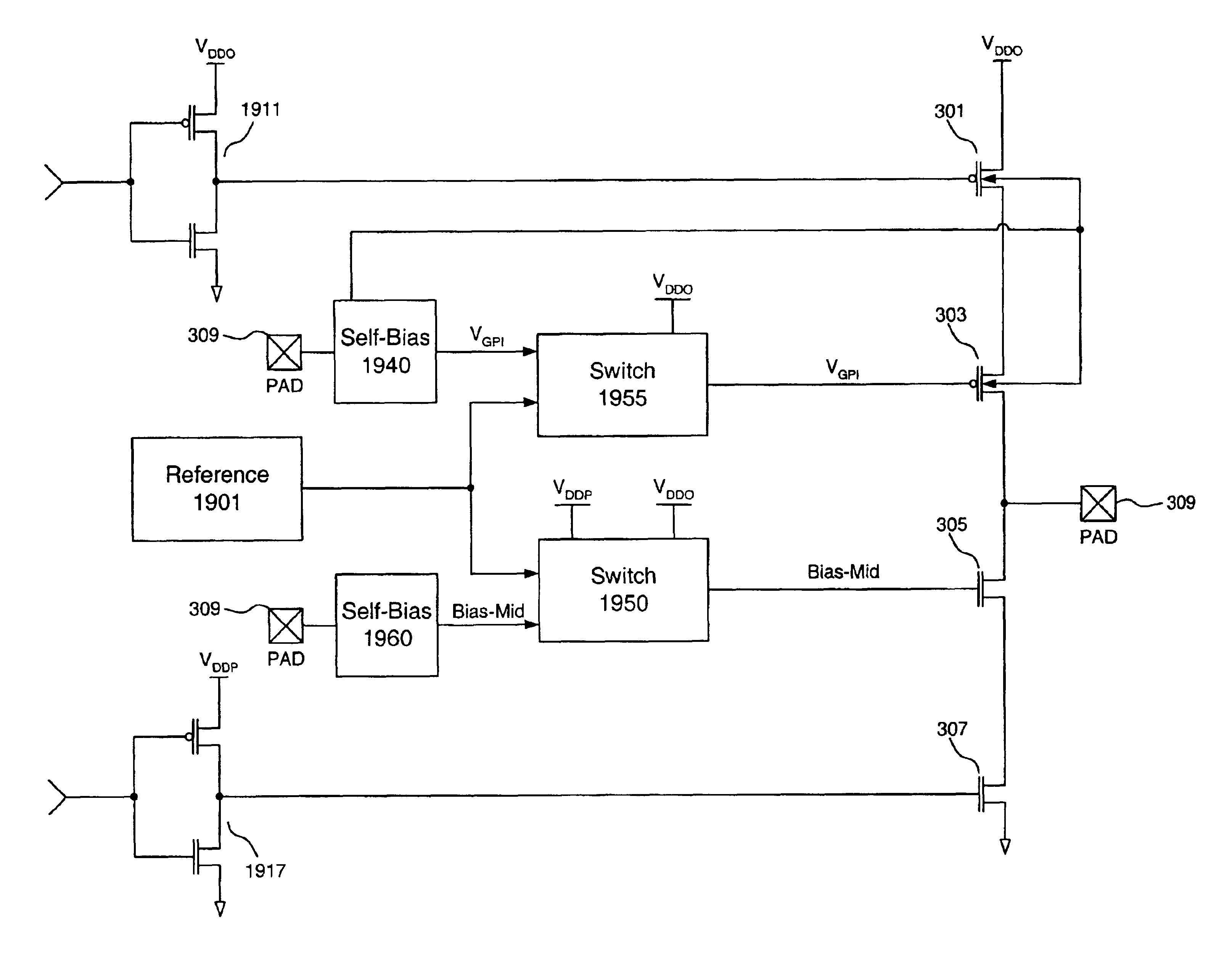
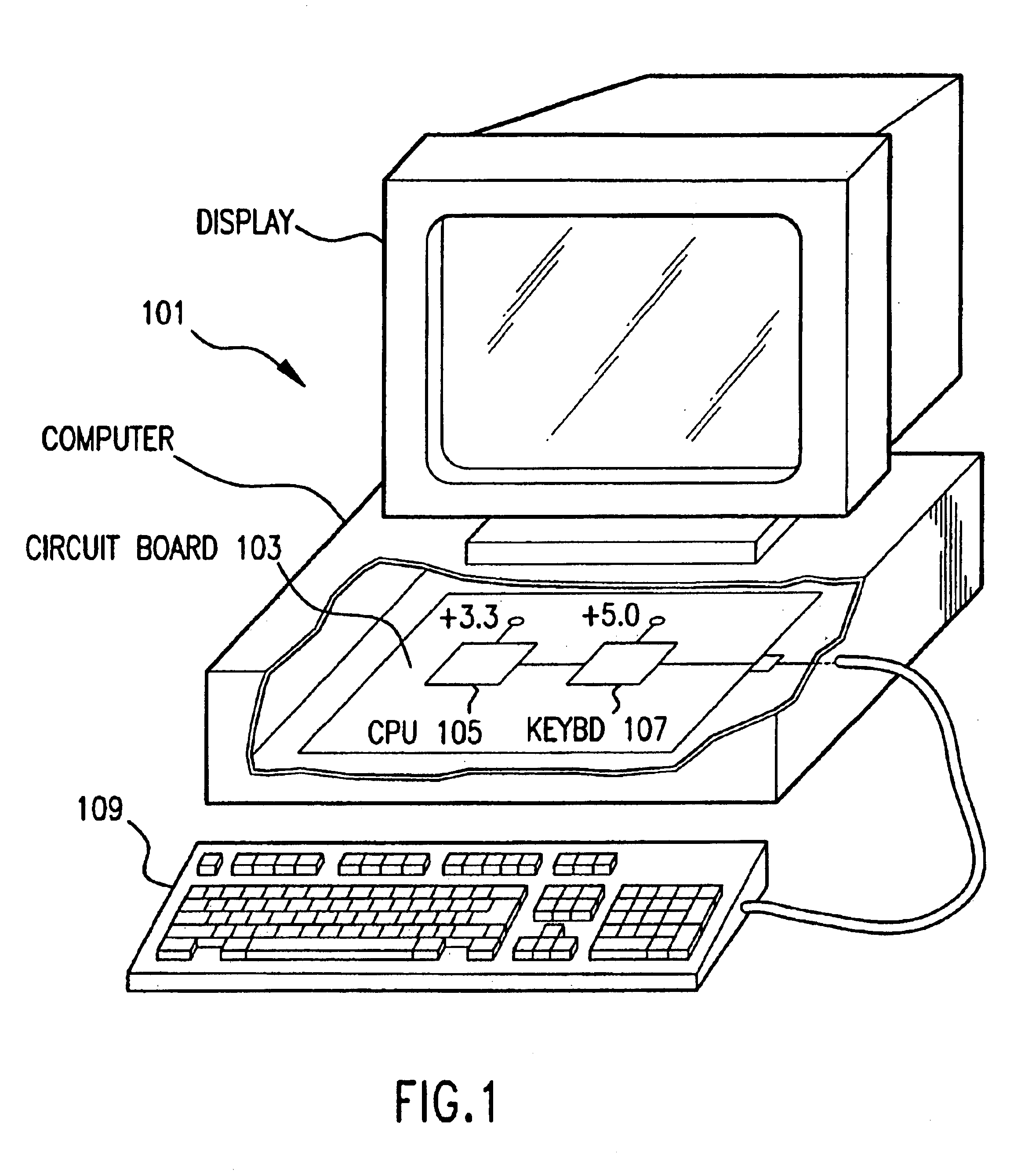
FIG. 1 is a graphic illustration of an exemplary environment in which embodiments of the invention may be utilized. In FIG. 1 a personal computer system is represented generally at 101. Within the computer system is circuit board 103 on which a CPU integrated circuit chip 105 is mounted. The CPU is a type which uses 3.3 volts as its supply voltage. A keyboard interface integrated circuit chip 107 is also mounted on circuit board 103. The keyboard interface integrated circuit uses a supply voltage of 5.0 volts. The CPU 105 is coupled to the Keyboard chip 107. The CPU 105 may be of a type which contains integrated devices that may be damaged by interfacing with a device having a higher supply voltage. Because of the disparity in supply voltages that may exist in such situations an output circuit which can compensate for the higher interface voltages may be useful.

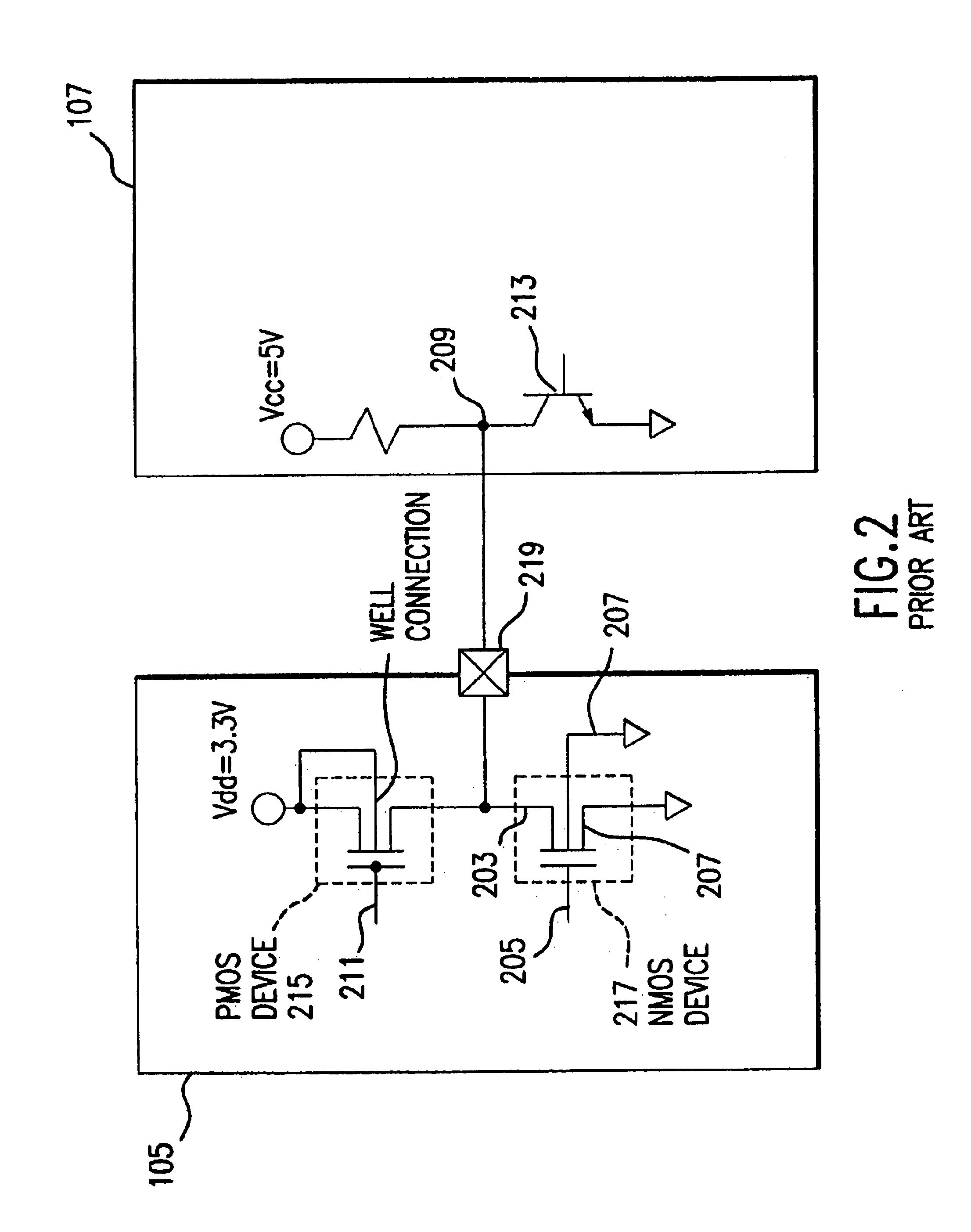
FIG. 2 is a graphical illustration of a prior art input output circuit and connection. A common input output circuit compri...


PUM


Abstract

An apparatus for providing bias voltages for input / output (I / O) connections on low voltage integrated circuits. In one embodiment, the invention comprises an I / O pad, a pull-down transistor device that has a protective transistor coupled to said I / O pad, and a pull-up transistor device that has a second protective transistor, coupled to said I / O pad. A first switch coupled to the first protective transistor is responsive to a first supply voltage, a second supply voltage, and a reference voltage. Likewise, a second switch coupled to the second protective transistor is responsive to the first supply voltage and the reference voltage. A first self-bias circuit is also coupled to the first switch, wherein said the self-bias circuit uses a voltage at said I / O pad to bias the first protective transistor when both of the first and second supply voltages are powered off. Likewise, a second self-bias circuit coupled to the second switch, wherein the second self-bias circuit also uses the voltage at the I / O pad and an output of the first self bias circuit, to bias the second protective transistor when the first supply voltage is powered off.

Description

BACKGROUND OF THE INVENTION1. Field of the InventionThe present invention relates to integrated circuits (ICs), such as interface circuits, that are designed having reduced feature sizes, for example, 0.13 μm. More particularly, the invention relates to ICs that include interfaces (such as input / output (I / O) circuits) that are capable of interfacing with comparatively high-voltage signals from other sources, for example a 3.3 volt IC interfacing with signals from a 5 volt IC, or any other disparate ranges. Moreover, the invention relates to integrated circuits in which the semiconductor devices are biased such that the stress across the gate-oxides and junctions, as well as the leakage currents, are maintained at tolerable levels.2. Related ArtThe trend in CMOS-based processing technology is to produce integrated circuit (IC) cores having a higher density of semiconductor devices, such as transistors, and faster clock rates than their predecessors. I / O circuits, which electrically c...

Claims


Application Information

Patent Timeline
Patent Type & Authority Patents(United States)
IPC IPC(8): H03K19/003
CPCH03K19/00315
Inventor AJIT, JANARDHANAN S.
Owner AVAGO TECH INT SALES PTE LTD
Why Eureka
Try Eureka