Pressure sensor and manufacturing method thereof
a capacitive pressure sensor and capacitive technology, applied in the direction of instruments, liquid/fluent solid measurement, specific gravity measurement, etc., can solve the problem of sensor diaphragm damage, etc., and achieve the effect of ensuring durability against overload
- Summary
- Abstract
- Description
- Claims
- Application Information
AI Technical Summary
Benefits of technology
Problems solved by technology
Method used
Image
Examples
example 1
[0045]The advantages of the invention will be explained specifically based on examples.
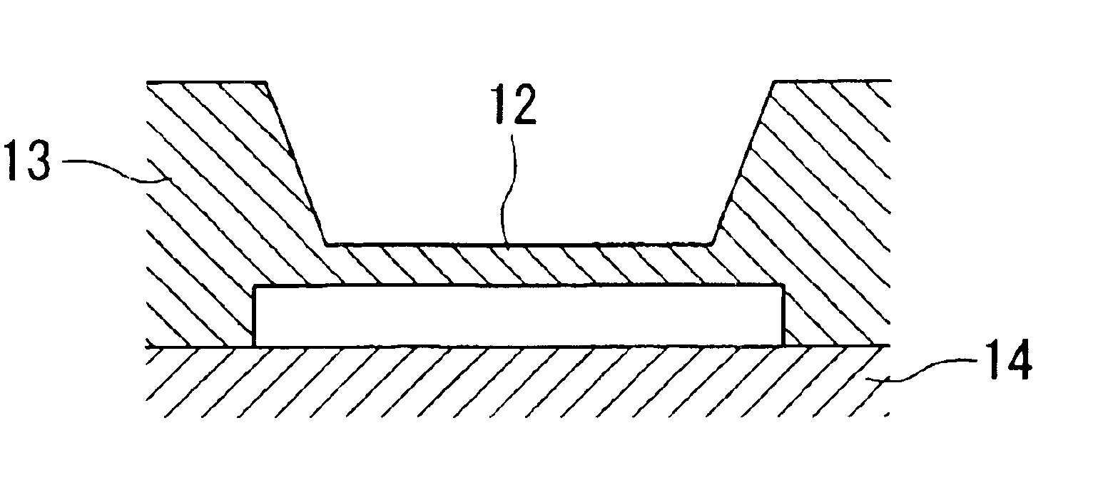
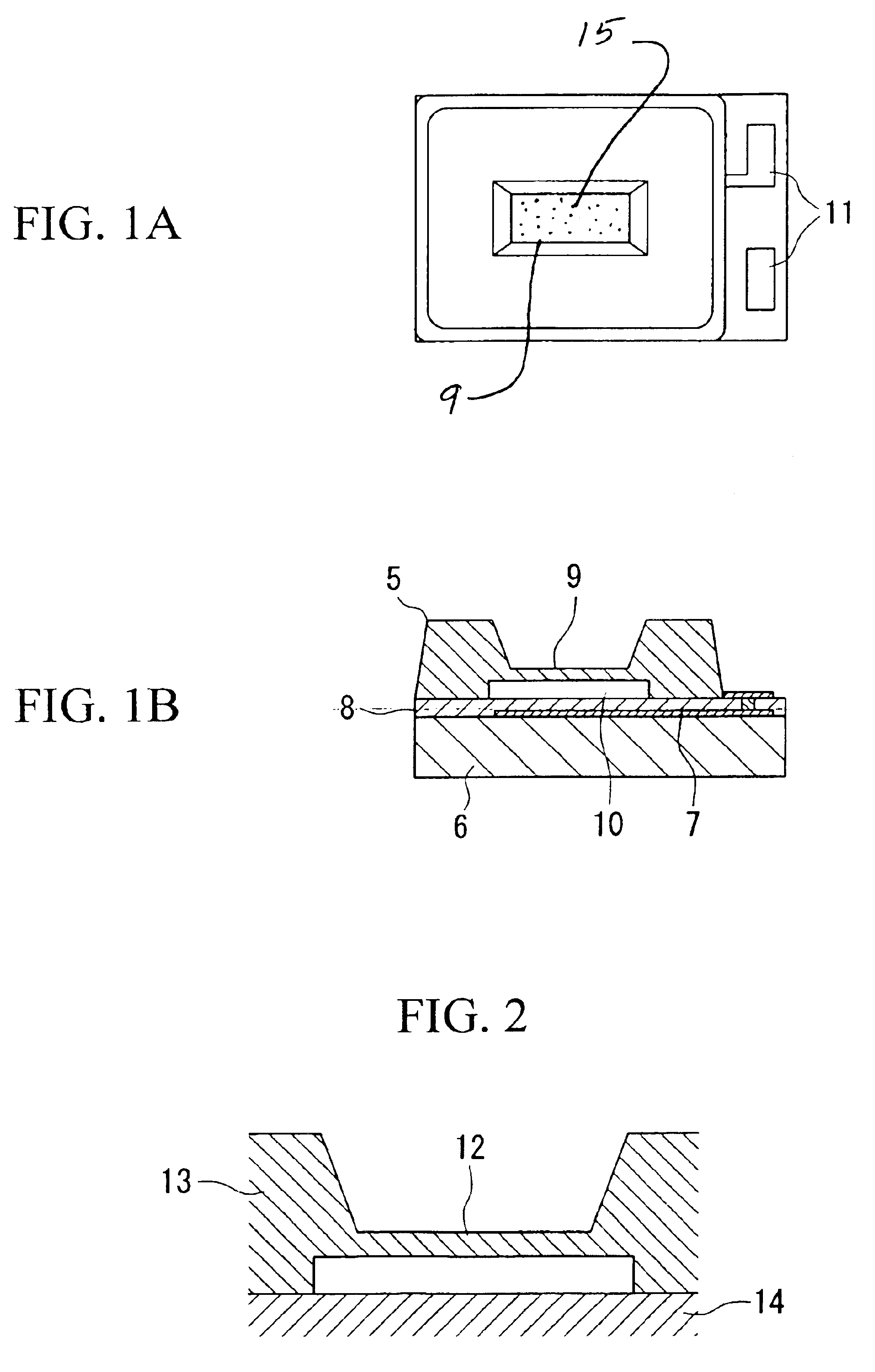
[0046]A touch mode capacitive pressure sensor having a silicon structure 5 comprising a diaphragm 9 bonded on a substrate 6, which a electrode 7 and a dielectric film 8 are provided on, such as that shown in FIGS. 1A and 1B, was manufactured.
[0047]During manufacturing, the electrode 7 comprising a Chromium thin-film and the dielectric film 8 comprising glass which covers the electrode 7 were provided on the substrate 6 comprising a glass plate; the electrode 7 and the dielectric film 8 have thickness of 0.1 μm and 0.4 μm respectively. The electrode 7 and the dielectric film 8 were formed in a series of processes, comprising film deposition using sputtering and patterning using lithography.
[0048]The diaphragm 9 is the opposite electrode of the lower electrode 7, and is made to function as an upper electrode by doping it with boron at high concentration. The shape of the diaphragm 9 in the top view ...
example 2
[0067]The effects of the present invention will be explained specifically based on an example.
[0068]A touch mode capacitive pressure sensor having the structure such as that shown in FIGS. 1A, 1B, and 2 was manufactured by the same sequence as in the first example, and was given a pressure durability test, in which breakage in the diaphragm were investigated after a constant pressure had been applied for a long period of time.
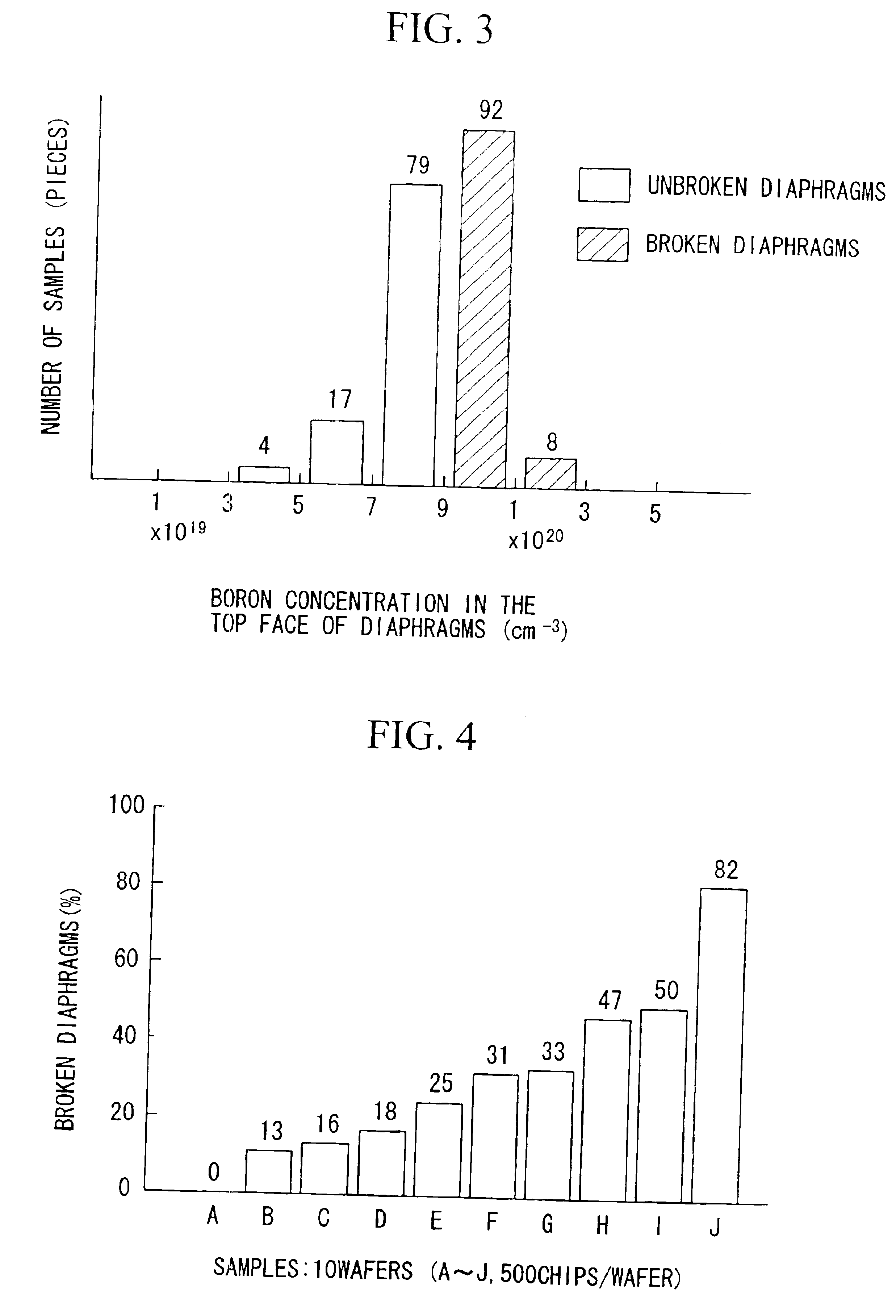
[0069]The test was carried out using wafers in their state prior to being cut into elements, and there were ten samples (ten wafers) A to J. Five-hundred sensor elements were arranged on each wafer.
[0070]After applying a pressure of 40 kgf / cm2 for a period of one hour, it was investigated whether there were any breakage in the diaphragms. FIG. 4 shows the distribution of the breakage of the wafers A to J which are sorted in the failed rate order. There was wide variation in the frequency from the wafers in which no diaphragms were broken to those in which 82% o...
PUM
| Property | Measurement | Unit |
|---|---|---|
| thickness | aaaaa | aaaaa |
| thickness | aaaaa | aaaaa |
| distance | aaaaa | aaaaa |
Abstract
Description
Claims
Application Information


