
Gallium indium nitride arsenide based epitaxial wafer, a hetero field effect transistor using the wafer, and a method of fabricating the hetero field effect transistor

a technology of gallium indium nitride arsenide and epitaxial wafer, which is applied in the direction of basic electric elements, electrical apparatus, semiconductor devices, etc., can solve the problems of insufficient carrier density, insufficient characteristic improvement, and inability to achieve sufficient carrier density, so as to improve electron mobility and operate at a high speed

Inactive Publication Date: 2005-03-01
PANASONIC CORP
View PDF8 Cites 9 Cited by
  • Summary
  • Abstract
  • Description
  • Claims
  • Application Information

AI Technical Summary

Benefits of technology

[0011]An object of the present invention is to provide a hetero field effect transistor capable of operating at a high speed by improving an electron mobility, a method of fabricating the transistor, and a transmitter-receiver.

Problems solved by technology

In the first prior art example, however, when the InAs layer 8 is inserted as described above, a lattice mismatching arises, thereby causing defects to occur if the InAs layer 8 has a film thickness not less than a critical film thickness.
Therefore, the thickness of the channel layer 8 needs to be less than the critical thickness, so that sufficient carrier density can not be realized and therefore the characteristic is not improved sufficiently.

Method used


Image

  • Gallium indium nitride arsenide based epitaxial wafer, a hetero field effect transistor using the wafer, and a method of fabricating the hetero field effect transistor
  • Gallium indium nitride arsenide based epitaxial wafer, a hetero field effect transistor using the wafer, and a method of fabricating the hetero field effect transistor
  • Gallium indium nitride arsenide based epitaxial wafer, a hetero field effect transistor using the wafer, and a method of fabricating the hetero field effect transistor

Examples


second embodiment

n">[0040]FIG. 9 is a cross-sectional view showing a structure of a hetero field effect transistor according to a first alternative example of the present invention;

third embodiment

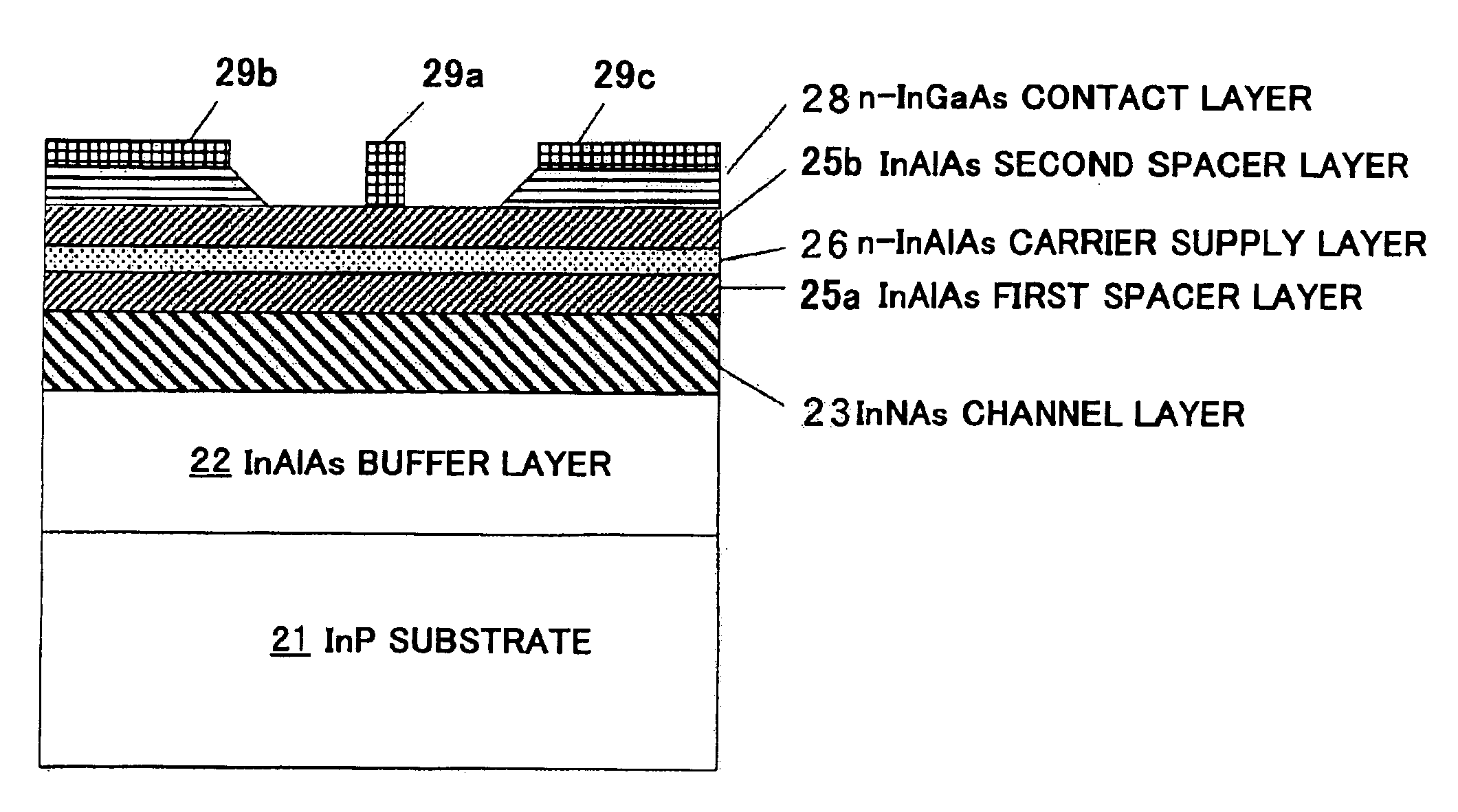
[0041]FIGS. 10A and 10B are views each showing a structure of a hetero field effect transistor according to the present invention, in which FIG. 10A is a cross-sectional view and FIG. 10B is a view showing an energy state in the vicinity of a channel layer in FIG. 10A;

[0042]FIG. 11 is a cross-sectional view showing a structure of a hetero field effect transistor according to a second alternative example of the second embodiment of the present invention;

fourth embodiment

[0043]FIG. 12 is a block diagram showing a structure of a transmitter-receiver according to the present invention;

[0044]FIG. 13 is a cross-sectional view showing a structure of a hetero field effect transistor according to a first prior art example; and

[0045]FIG. 14 is a cross-sectional view showing a structure of a hetero field effect transistor according to a second prior art example.

DETAILED DESCRIPTION OF THE PREFERRED EMBODIMENTS

[0046]Hereinafter, embodiments of the present invention will be described with reference to drawings.

[0047]{Concept of the Present Invention}

[0048]First of all, a concept of the present invention will be described.

[0049]A hetero field effect transistor of the present invention is characterized by a structure in which GaInNAs comprising a predetermined range of composition ratio of Ga and N is formed as a channel layer on an InP substrate. In the present invention, GaInNAs is comprised of InNAs in an embodiment in which no Ga is contained. In other words...


PUM


Abstract

A hetero field effect transistor according to the present invention comprises an InP substrate, a channel layer provided on the InP substrate with a buffer layer disposed between the InP substrate and the channel layer, a spacer layer constituted by a semiconductor having a band gap larger than that of the channel layer formed to hetero-join to the channel layer, and a carrier supply layer formed to be adjacent to the spacer layer, wherein the channel layer comprises a predetermined semiconductor layer constituted by a compound semiconductor represented by a formula GaxIn1−xNyA1−y in which A is As or Sb, composition x satisfies 0≦x≦0.2, and composition y satisfies 0.03≦y≦0.10.

Description

[0002]This is a continuation application under 35 U.S.C 111(a) of pending prior International application No. PCT / JP03 / 13747, filed on Oct. 28, 2003.BACKGROUND OF THE INVENTION[0003]1. Technical Field[0004]The present invention relates to a hetero field effect transistor using a gallium indium nitride arsenide based epitaxial wafer, to a method of fabricating the hetero field effect transistor, and to a transmitter-receiver using the hetero field effect transistor.[0005]2. Related Art[0006]A hetero field effect transistor such as a high electron mobility transistor (HEMT) is a compound semiconductor device using a two-dimensional electron gas formed by a hetero structure.[0007]FIG. 13 shows a conventional HEMT as a first prior art example of such HEMT, comprising an InAlAs carrier supply layer / an InGaAs channel layer / an InAlAs buffer layer formed on an InP substrate. In FIG. 13, reference numerals 1 to 7 denote an electrode metal, an n+-InGaAs cap layer, an n-InAlAs carrier supply l...

Claims


Application Information

Patent Timeline
IPC IPC(8): H01L21/02H01L29/66H01L29/778H01L21/335H01L29/20H01L29/02H01L29/812H01L21/338
CPCH01L29/201H01L29/7785H01L29/7784H01L29/66462H01L29/2003
Inventor OTSUKA, NOBUYUKIMIZUNO, KOICHIYOSHII, SHIGEOSUZUKI, ASAMIRA
Owner PANASONIC CORP
Learn More