Schottky diode having overcurrent protection and low reverse current

a diode and reverse current technology, applied in the field of schottky diodes, can solve the problems of reducing the electrical field strength at the rated voltage, reducing the forward voltage of the schottky diode, and causing the diode to be significantly more forward voltage, so as to achieve good resistance to overcurrents and low forward voltage

Active Publication Date: 2005-03-01
INFINEON TECH AG
View PDF3 Cites 91 Cited by
  • Summary
  • Abstract
  • Description
  • Claims
  • Application Information

AI Technical Summary

Benefits of technology

The object of the present invention is thus to provide a Schottky diode which is distingui

Problems solved by technology

This means that a considerably increased leakage current occurs in Schottky diodes even considerably below the theoretical breakdown field strength of its semiconductor material.
All of these measures for reducing the electrical field strength at the rated voltage lead, however, to the forward voltage of the Schottky diode being considerably greater than it would need to be without the measures taken to overcome the surface problems explained above.
A further problem, in particular in the case o

Method used


Image

  • Schottky diode having overcurrent protection and low reverse current
  • Schottky diode having overcurrent protection and low reverse current
  • Schottky diode having overcurrent protection and low reverse current

Examples


Embodiment Construction

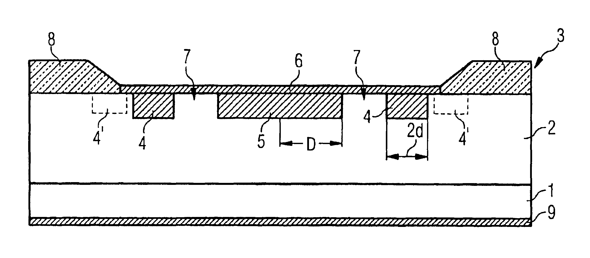
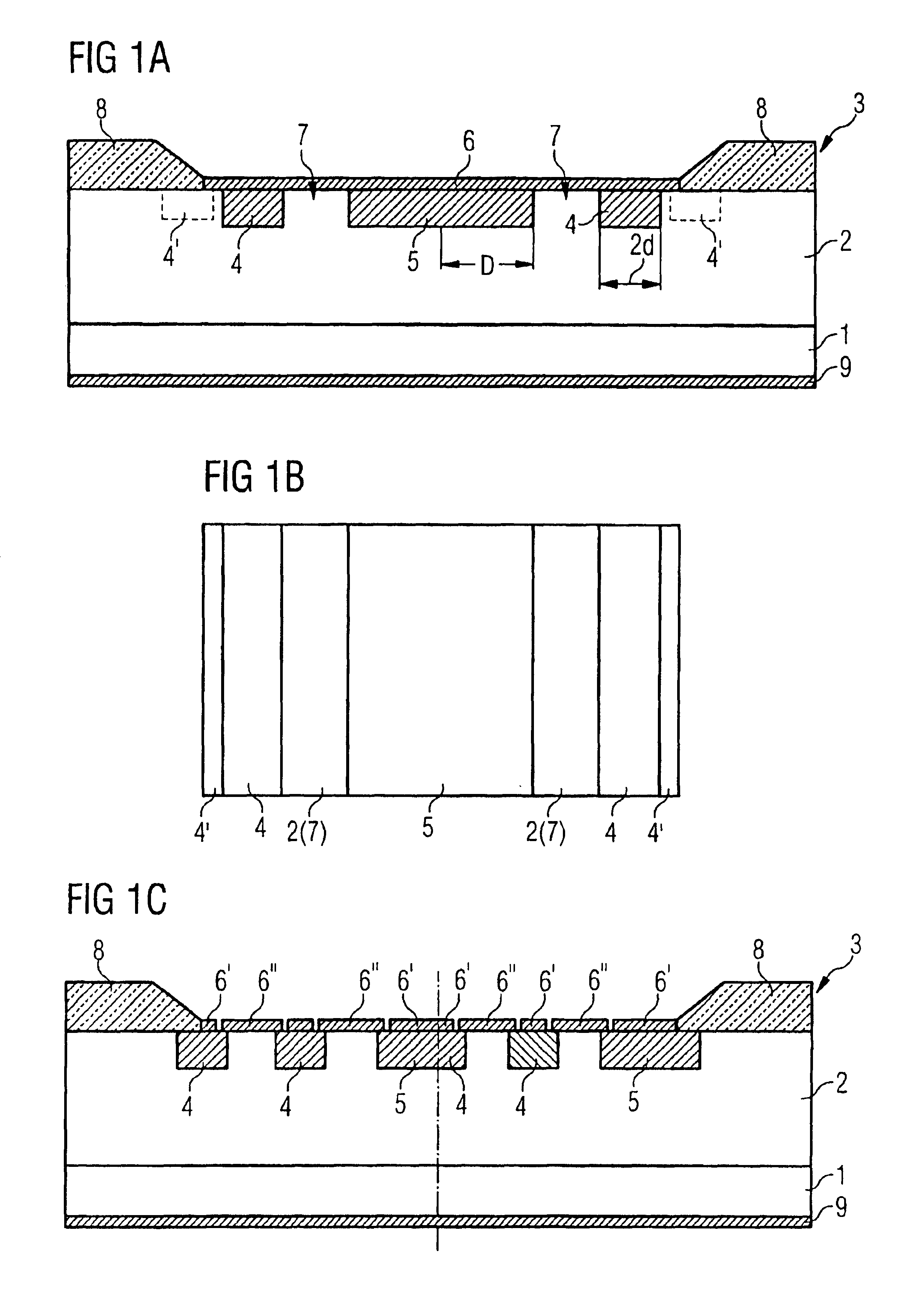
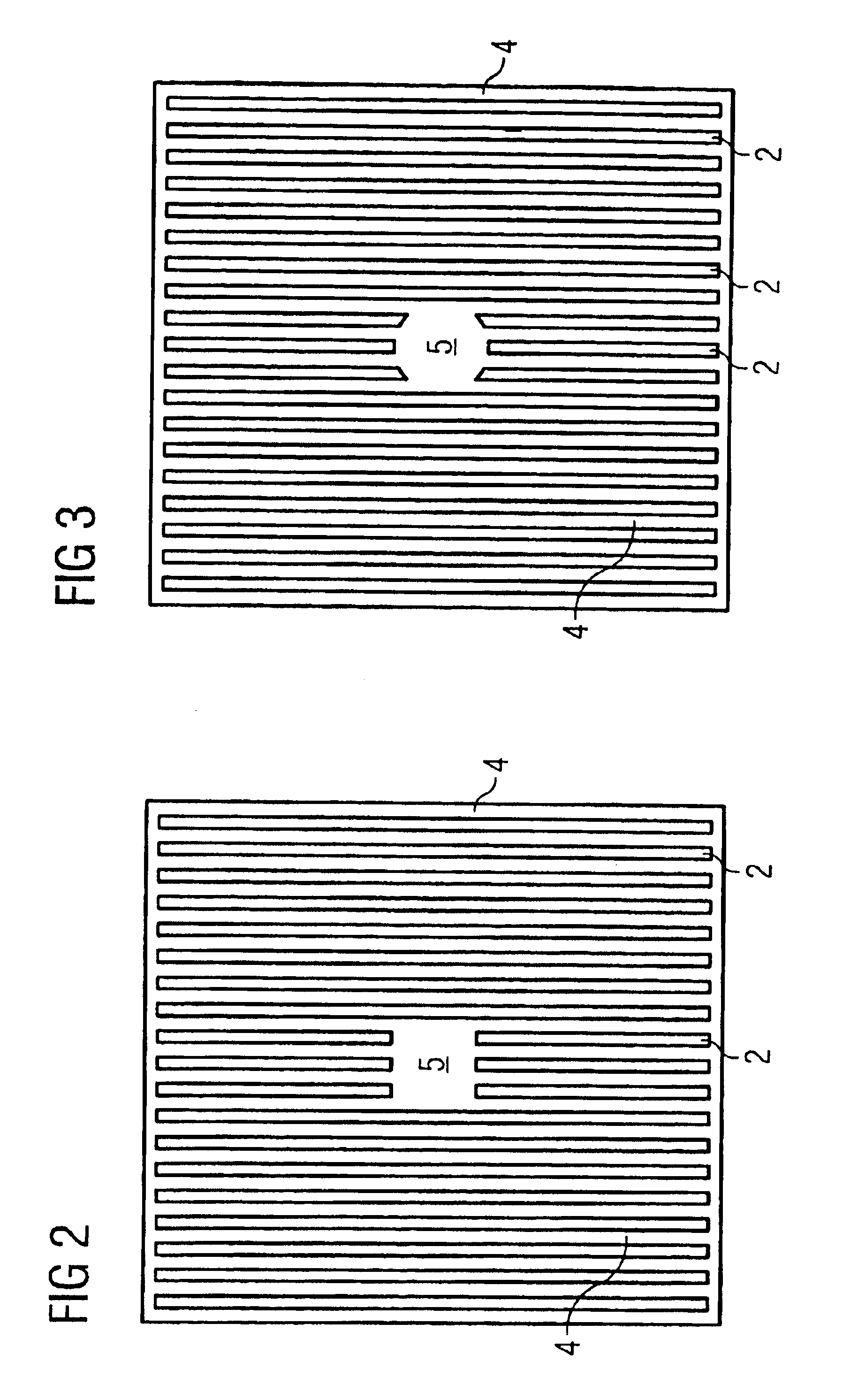
FIG. 1A shows, on an n-doped silicon carbide substrate 1, an n-doped silicon carbide layer 2, which is, for example, deposited epitaxially and in whose surface area p-doped regions 4, 5 which are in the form of strips are incorporated. The width of the region 5 which is in the form of strips is in this case greater by a factor of 3 than the width of the regions 4 which are in the form of strips.

The edge should preferably be p-conductive. This can be achieved, for example, by means of an additional p-conductive region 4′, which may be cohesive with the region 4 closest to it, or alternatively may be separate from it. However, it is likewise also possible to provide a region 4 directly as the edge. The region 4′ may also be doped more strongly or more weakly than the region 4.

Even though only one broad region 5 and two narrow regions 4 are provided in FIGS. 1A and 1B, it is self-evident that considerably more narrow regions 4 as well as more than one broad region 5 may be provided.

The...


PUM


Abstract

The invention relates to a Schottky diode in which p-doped regions (4, 5) are incorporated in the Schottky contact area. At least one (5) of these regions (4, 5) has a greater minimum extent, in order to initiate a starting current.

Description

FIELD OF THE INVENTIONThe present invention relates to a Schottky diode having a semiconductor body of a first conductance type, having a Schottky contact which is provided on the semiconductor body, and having two or more regions of the other conductance type, which are located in the semiconductor body underneath the Schottky contact and are at least partially adjacent to the Schottky contact.BACKGROUNDConventional Schottky diodes have the characteristic that, when they are loaded with a voltage in the reverse direction, the greatest electrical field strength occurs directly adjacent to the surface of the Schottky contact. This means that a considerably increased leakage current occurs in Schottky diodes even considerably below the theoretical breakdown field strength of its semiconductor material. In addition to silicon, silicon carbide (SiC), for example, may also be used as the semiconductor material.As a result of the above characteristic, Schottky diodes are in practice desig...

Claims


Application Information

Patent Timeline
IPC IPC(8): H01L29/66H01L29/02H01L29/06H01L29/872H01L29/24
CPCH01L29/0692H01L29/872H01L29/1608H01L29/0619
Inventor WILLMEROTH, ARMIN
Owner INFINEON TECH AG
Why Eureka
Try Eureka