Method of fabricating integrated electronic chip with an interconnect device

a technology of interconnecting devices and electronic chips, which is applied in the direction of manufacturing tools, solid-state devices, basic electric elements, etc., can solve the problems of increasing the density of the respective device elements, and increasing the complexity of the device. complexity, which is a special challenge for the device packaging technologis

Active Publication Date: 2005-03-08
VEECO INSTR
View PDF19 Cites 83 Cited by
  • Summary
  • Abstract
  • Description
  • Claims
  • Application Information

AI Technical Summary

Benefits of technology

According to an additional aspect of the invention, an integrated structure is provided which includes a semiconductor device and connector structures for connecting the semiconductor device to a motherboard. Furthermore, the integrated structure includes a first layer having a first set of conductors disposed therein; the first set of conductors connect to bonding pads disposed on the lower surface of the layer. The bonding pads are spaced with respect to each other with a first spacing distance in accordance with a required spacing of connections to the motherboard. A second layer, facing the first layer, is disposed on the semiconductor device and in contact therewith; the second layer has a second set of conductors disposed therein con

Problems solved by technology

Electronic devices are continuing to become more complex with each generation, while at the same time their respective device elements are becoming smaller.
This trend toward greater device density and complexity presents special challenges for the device packaging technologist.
An example of a complex, large-scale chip which presents a challenge for packaging technology is the sy

Method used


Image

  • Method of fabricating integrated electronic chip with an interconnect device
  • Method of fabricating integrated electronic chip with an interconnect device
  • Method of fabricating integrated electronic chip with an interconnect device

Examples


first embodiment

ing Layer Using Stud / Via Connections

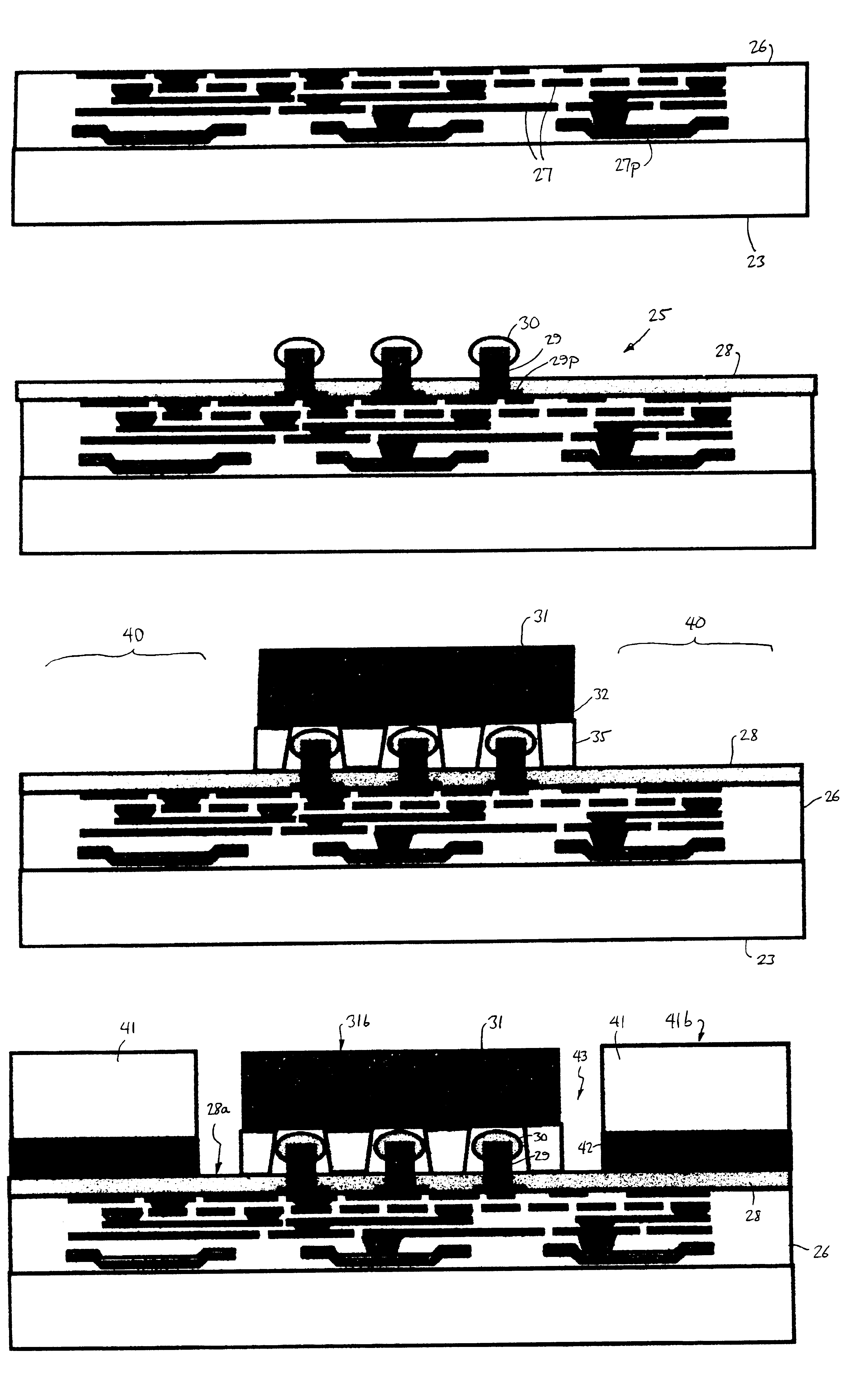
The interconnect wiring 27 (preferably Cu) is embedded in a dielectric layer 26 (typically polyimide or an oxide) on a transparent substrate 23 (see FIG. 2A). Substrate 23 is typically made of glass such as boro-float glass and has a size of 200 mm in diameter, commensurate with wafer sizes used in manufacturing. Although layer 26, including conductors 27, is shown as a single layer, it will be appreciated that for ease of manufacturing it is often designed and fabricated as a multilayer structure. The number of levels of wiring in layer 26 depends on the connection density required to match with the chip connections; typically 3 to 5 metal layers are required. The Cu conductors 27 connect to bonding pads 27p which typically are formed of Ni (but may also be Cu, Au, Co or a combination thereof). The bonding pads 27p have a spacing in accordance with a required spacing of connections to a motherboard. For example, if conductors 27 are to be connect...

second embodiment

ng Layer Using C4 Connections

In this embodiment, the connection between chip 31 and interconnect wiring 27 is realized using conventional C4 connectors. As shown in FIG. 6A, chip 61 has BEOL metal wiring layers embedded in a dielectric layer 62, with the last metal layer connecting to pads 63 on which C4 solder balls 64 are formed. Interconnect wiring 67 (preferably Cu) is embedded in a dielectric layer 66 (typically polyimide or an oxide) on a transparent substrate 68. The interconnect wiring also connects to bonding pads 67p, as in the first embodiment (see FIG. 6B; compare FIG. 2A). A stiffener 41 is prepared with an adhesive layer 42 on the top thereof, then flipped over and joined to layer 66, to form the structure of FIG. 6C. As in the first embodiment, the stiffener has a hole in its center slightly larger than chip 61.

The chip is then joined to the interconnect wiring layer by a conventional C4 chip join process (FIG. 6D). The entire gap between the chip and the stiffener, i...


PUM

PropertyMeasurementUnit
Expansion enthalpyaaaaaaaaaa

Abstract

A method is described for forming an integrated structure, including a semiconductor device and connectors for connecting to a motherboard. A first layer is formed on a plate transparent to ablating radiation, and a second layer on the semiconductor device. The first layer has a first set of conductors connecting to bonding pads, which are spaced with a first spacing distance in accordance with a required spacing of connections to the motherboard. The second layer has a second set of conductors connecting to the semiconductor device. The first layer and second layer are connected using a stud/via connectors having spacing less than that of the bonding pads. The semiconductor device is thus attached to the first layer, and the first set and second set of conductors are connected through the studs. The interface between the first layer and the plate is ablated by ablating radiation transmitted through the plate, thereby detaching the plate. The connector structures are then attached to the bonding pads. This method permits fabrication of a high-density packaged device with reduced cost.

Description

BACKGROUND OF INVENTIONThis invention relates to the manufacture of electronic device modules which include high-performance semiconductor devices (including CMOS logic devices, DRAM memory devices and the like) and interconnections between those devices. In particular, the invention relates to fabrication of high-density chip interconnections with improved reliability and reduced cost.Electronic devices are continuing to become more complex with each generation, while at the same time their respective device elements are becoming smaller. This trend toward greater device density and complexity presents special challenges for the device packaging technologist. Semiconductor devices at present are manufactured with either wire bond pads or C4 pads to connect such devices to the next level interconnect; this is generally termed the first level of packaging.The packaging sector has for a number of years represented the primary constraint on improving system speed for many semiconductor...

Claims


Application Information

Patent Timeline
IPC IPC(8): H01L23/498H01L23/16H01L23/24H01L23/48H01L21/60H01L21/68
CPCH01L21/6835H01L23/24H01L23/49811H01L23/49816H01L23/49822H01L23/49827H01L23/49833H01L23/562H01L24/81H01L23/49838H01L2221/68345H01L2221/68381H01L2224/131H01L2224/13111H01L2224/13147H01L2224/13155H01L2224/81001H01L2224/81136H01L2224/81191H01L2224/81192H01L2224/81801H01L2224/83101H01L2224/83192H01L2224/83194H01L2224/83365H01L2224/83907H01L2924/01029H01L2924/01033H01L2924/01057H01L2924/01078H01L2924/01079H01L2924/01082H01L2924/15153H01L2924/1517H01L2924/15311H01L2924/15312H01L2924/15313H01L2924/18161H01L2924/19041H01L2924/00013H01L2924/01005H01L2924/01006H01L2924/01047H01L2924/0105H01L2924/01074H01L2924/014H01L2224/16225H01L2224/81005H01L2224/13099H01L2924/00H01L2224/29099H01L2924/351H01L2924/12042H01L2224/05573H01L2224/05568H01L2924/00014H01L23/16H01L2224/05599
Inventor POGGE, H. BERNHARDPRASAD, CHANDRIKAYU, ROY
Owner VEECO INSTR
Why Eureka
Try Eureka