Circuit and method for regenerating reset and clock signals and high-speed digital system incorporating the same

Active Publication Date: 2005-03-08
SAMSUNG ELECTRONICS CO LTD
View PDF5 Cites 11 Cited by
  • Summary
  • Abstract
  • Description
  • Claims
  • Application Information

AI Technical Summary

Benefits of technology

[0016]The system of the invention can further include a counter circuit for generating a count of a number of cycles of the external clock signal. Also, a first comparator circuit can compare the count with a first threshold and initiate the masking period when the count reaches the first threshold. A second comparator circuit can compare the count with a second threshold and terminate the masking period when the count reaches the second threshold. A third comparator circuit can compa

Problems solved by technology

In this case, it is difficult to ensure that a flip-flop circuit will latch a value applied to the data input terminal D thereof.
Under this condition, it is also difficult to ensure the flip-flop circuit will latch a value applied to the data input terminal D thereof.
As a result, it is d

Method used


Image

  • Circuit and method for regenerating reset and clock signals and high-speed digital system incorporating the same
  • Circuit and method for regenerating reset and clock signals and high-speed digital system incorporating the same
  • Circuit and method for regenerating reset and clock signals and high-speed digital system incorporating the same

Examples


Embodiment Construction

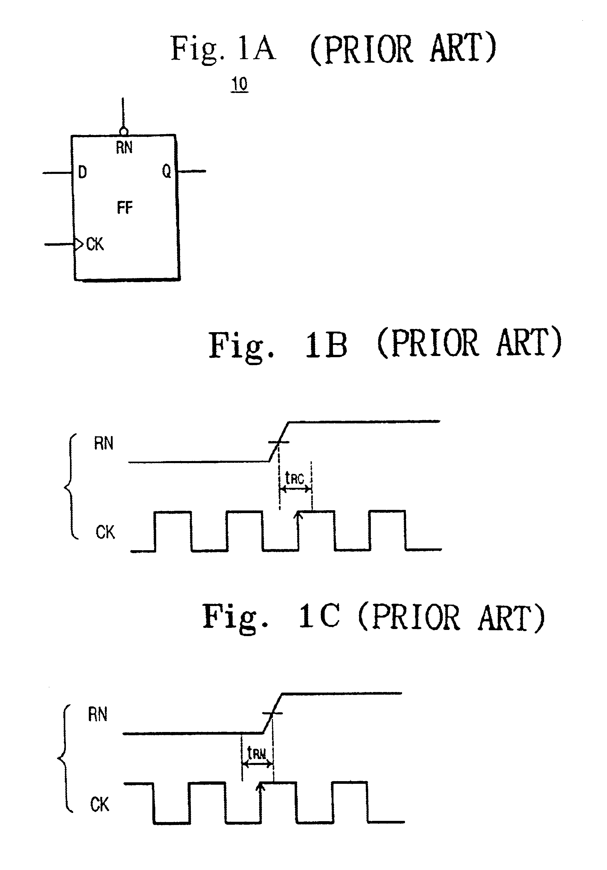
>[0031]FIG. 8 is a flowchart illustrating operation of a reset and clock regenerator circuit of a semiconductor device according to the present invention.

[0032]FIG. 9 is a timing diagram illustrating operation of a reset and clock regenerator circuit of a semiconductor device according to the present invention.

[0033]FIG. 10 is a timing diagram illustrating an inadvertent pulse or glitch in an internal clock signal when a delay circuit in FIG. 4 is not used.

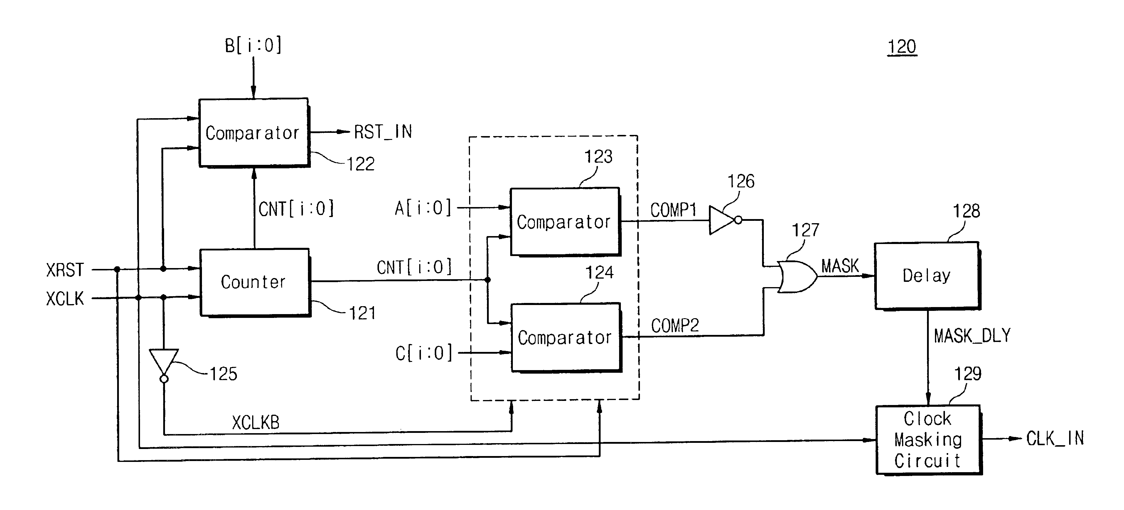
[0034]FIG. 11 is a block diagram showing a semiconductor device according to another embodiment of the present invention.

[0035]FIG. 12 is a block diagram showing a semiconductor device according to another embodiment of the present invention.

DETAILED DESCRIPTION OF PREFERRED EMBODIMENTS OF THE INVENTION

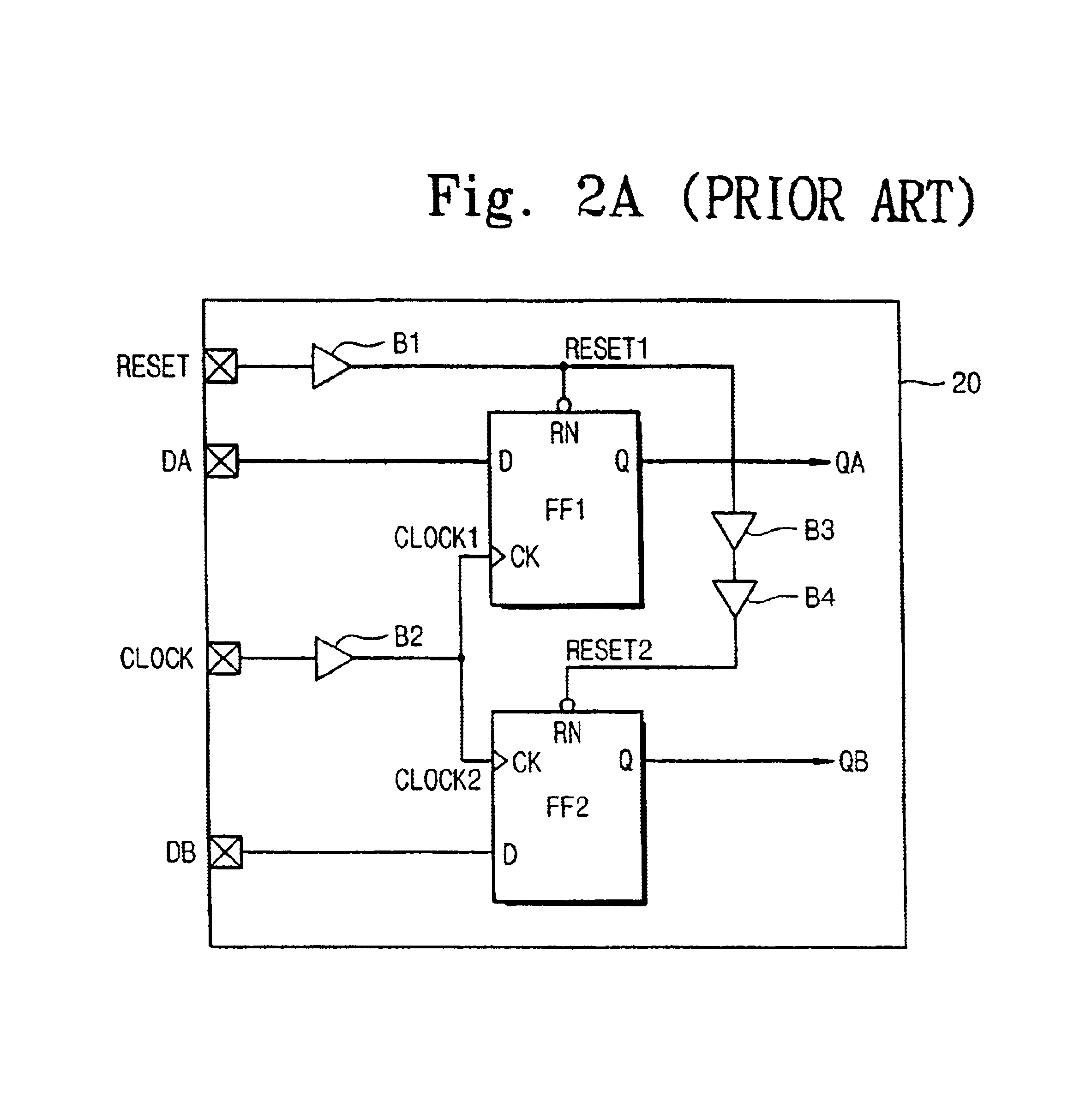
[0036]A block diagram of a semiconductor device according to the present invention is illustrated in FIG. 3. Referring to FIG. 3, a semiconductor device 100 of the present invention is supplied with an external clock signal, e.g., a...


PUM


Abstract

An apparatus and method for regenerating reset and clock signals and a high-speed digital system using the apparatus and method are provided. In the regenerating circuit of the invention, a clock circuit receives an external clock signal and generates there from an internal clock signal, which is forwarded to a plurality of clocked circuits such as, for example, D flip-flops. A reset circuit receives an external reset signal and generates therefrom an internal reset signal, which is forwarded to the clocked circuits to reset the clock circuits. A clock masking circuit masks the internal clock signal for a masking period such that the clocked circuits are not clocked during the masking period. The high-speed digital system of the invention includes a plurality of function blocks coupled on a bus. The reset and clock regenerating circuit of the invention generates internal reset and clock signals from externally applied reset and clock signals.

Description

RELATED APPLICATIONS[0002]This application claims the priority of Korean Patent Application No. 2002-0080115, filed Dec. 16, 2002, in the Korean Intellectual Property Office, the contents of which are incorporated herein in their entirety by reference.[0003]1. Field of the Invention[0004]The present invention relates to a semiconductor device with external reset and clock signals and a high-speed digital system incorporating the same.[0005]2. Background of the Invention[0006]Flip-flop circuits are essential elements that are used in almost all integrated circuits. Among other functions, flip-flop circuits are used to store data as results of computations carried out by digital circuits, or they sequentially arrange data in an integrated circuit to utilize computations. Binary flip-flops are capable of storing two signal levels, that is, logic high and logic low. In general, all signals to flip-flops have the two possible logic levels. One example of such a flip-flop is illustrated i...

Claims


Application Information

Patent Timeline
IPC IPC(8): G06F1/24G06F1/10G06F1/04G11C7/00
CPCG06F1/24G06F1/10G11C7/00
Inventor JOO, JIN-TAE
Owner SAMSUNG ELECTRONICS CO LTD
Why Eureka
Try Eureka