Tunable optical wavelength filters and multi-level optical integrated circuits

a wavelength filter and multi-level technology, applied in the field of optical telecommunication network apparatus and methods, can solve the problems of affecting the quality factor, q, of the cavity as well, and it is difficult to maximize the performance of such prior art devices by phase matching the waveguide, and achieves accurate control of the gap size, reduce the horizontal surface area, and improve the coupling efficiency of a tunable resonant optical wavelength filter.

Inactive Publication Date: 2005-03-08
BLAIR STEVEN M +1
View PDF35 Cites 62 Cited by
  • Summary
  • Abstract
  • Description
  • Claims
  • Application Information

AI Technical Summary

Benefits of technology

The tunable resonant optical wavelength filter of the present invention has a number of advantages over prior art devices. In particular, the resonant cavity (which may be in a disk, ring, racetrack, or similar geometries) lies, preferably, on top of or beneath the input and output waveguides, vertically separated by a material or region of lower refractive index. The vertical arrangement allows more accurate control over the gap size during manufacture than does the traditional side coupling arrangement of the prior art, which requires the performance of very precise and high resolution lithography during manufacture in order to control the gap spacing, which strongly affects the coupling between the cavity and waveguides, and therefore affects the quality factor, Q, of the cavity as well. In the vertical arrangement of the present invention, the gap separation is controlled by a thin film deposition, implantation, or diffusion process, which can be more accurately controlled so that coupling efficiency and Q can be controlled. Also, since the waveguides and cavity are separated vertically, they may be made of different materials and may be of different thicknesses, either of which allows additional flexibility in maximizing device performance in terms of phase matching the waveguide and cavity modes for efficient coupling.
Additionally, there may be a lateral offset between the cavity and the input and output waveguides. The lateral offset allows improved overlap between the mode of the waveguides and the desired mode of the cavity. Accordingly, the cavity may either overhang or underhang the waveguides. When the cavity overhangs the waveguides, higher-order radial modes of the cavity may be excited. These higher-order modes are less susceptible to scattering losses. When the cavity underhangs the waveguides, a more efficient coupling into the fundamental cavity mode may be obtained from the waveguide. Both overhanging and underhanging arrangements of the cavity and the waveguides may be used to control the resonance bandwidth of the cavity.
In addition, the vertical geometry of the present invention makes the implementation of tuning mechanisms easier by enabling the avoidance of interference with the coupling waveguides. Finally, the vertical structure may be extended to include multi-layer optical circuits using a planarization technique.
Another object of the present invention is to reduce the horizontal surface area of a tunable resonant optical wavelength filter.
Sill another object of the present invention is to allow accurate control over the gap size of a tunable resonant optical wavelength filter during manufacture.
Still another object of the present invention is to improve the quality factor and coupling efficiency of a tunable resonant optical wavelength filter.

Problems solved by technology

The prior art devices have, however, a few disadvantages and / or shortcomings.
First, many of the prior art devices utilize side coupling, with the cavity and waveguides lying in the same plane.
The manufacture of such a side coupled device requires very precise and high resolution lithography to be performed in order to control the gap spacing, which strongly affects the coupling between the cavity and waveguides, and therefore affects the quality factor, Q, of the cavity as well.
Second, because the cavity and waveguides of such prior art devices are in the same plane, they are typically manufactured from the same material and have the same thickness.
As a consequence, it is difficult to maximize performance of such prior art devices by phase matching the waveguides and cavity.
Third, electrode placement in the planar prior art devices may be limited due to the side coupling arrangement of the waveguides and cavity and, hence, may interfere with the modes of the waveguides and, thereby introduce a potential source of loss.
Fourth, the resonant cavities have only been considered as lying in the same plane, thereby limiting circuit flexibility and the density at which optical integrated circuits may be made.
Finally, it is difficult to match the modal profile of the coupling waveguides to the desired mode of the cavity when using side coupling.

Method used


Image

  • Tunable optical wavelength filters and multi-level optical integrated circuits
  • Tunable optical wavelength filters and multi-level optical integrated circuits
  • Tunable optical wavelength filters and multi-level optical integrated circuits

Examples


second embodiment

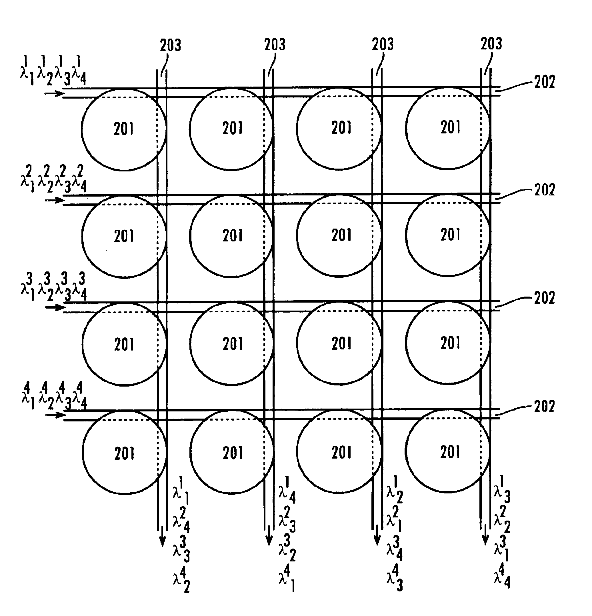
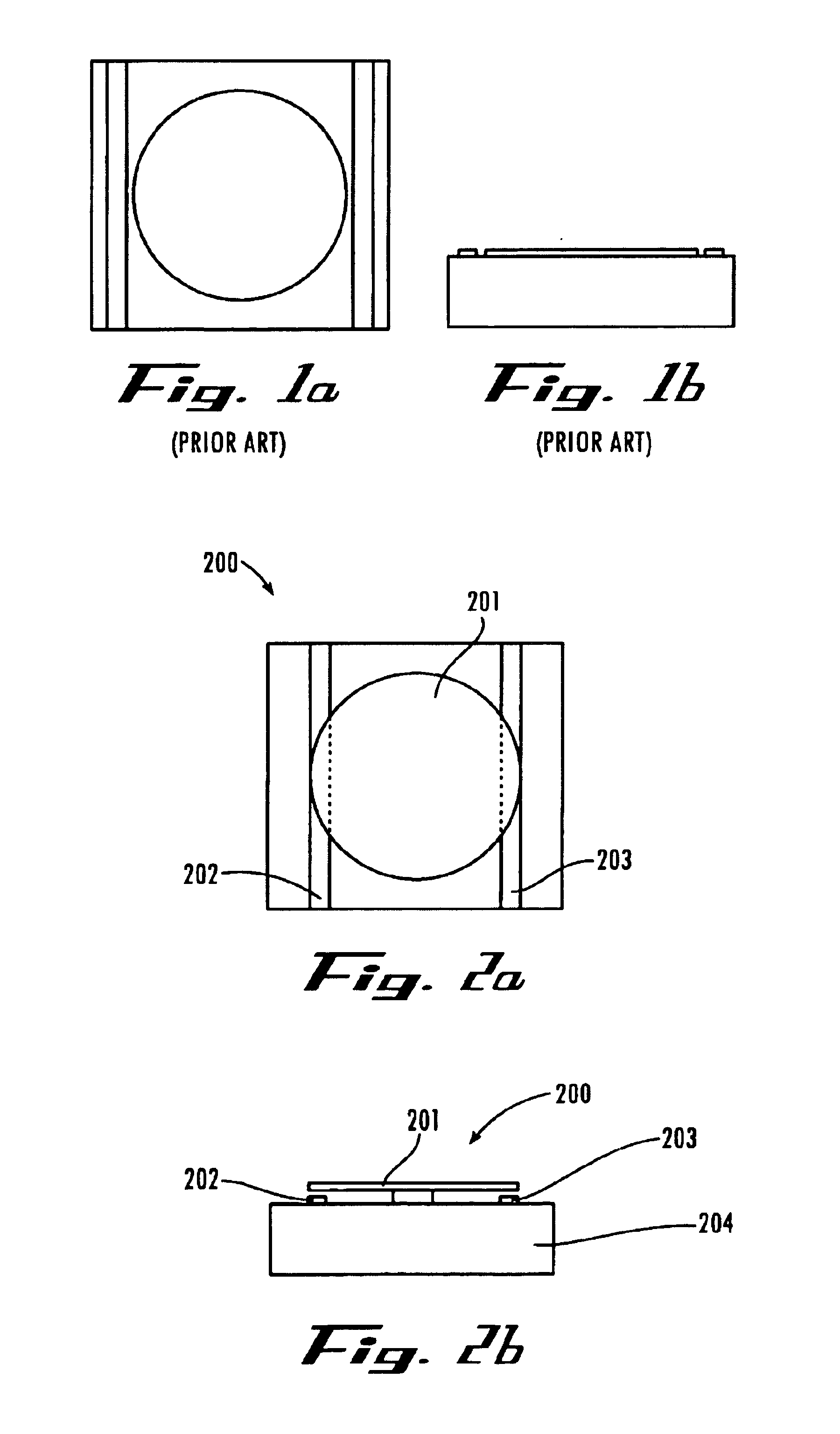
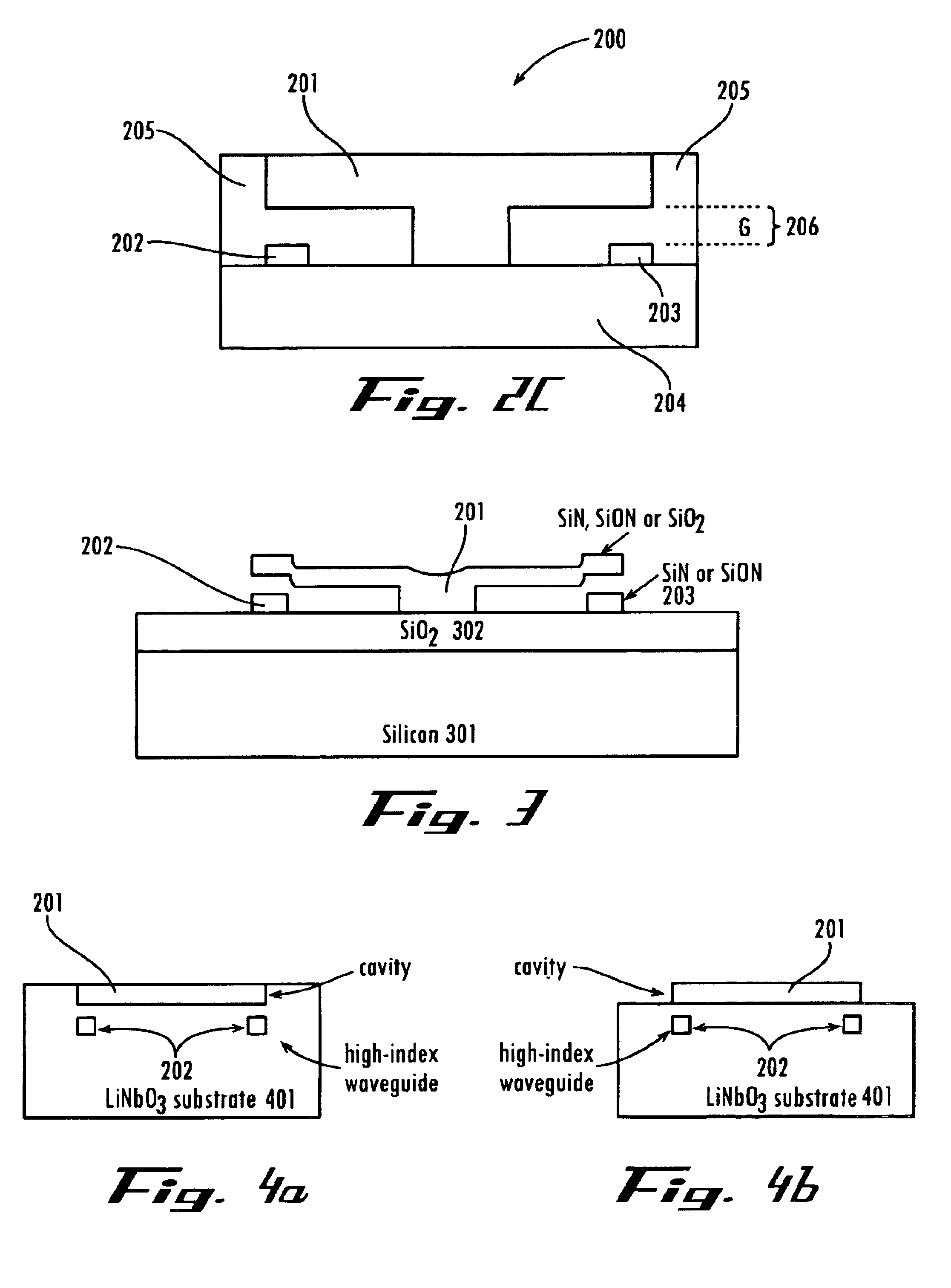
the present invention has the advantages that the resonant cavity 201 may be made in a crystalline material that is electro-optic, while the waveguide 202, 203 structures may be made of a different material in which very low loss waveguides 202, 203 may be fabricated. In addition, the different materials (with different refractive indices) allow greater control over coupling into and out of the resonant cavity 201. Finally, placement of the waveguides 202, 203 on top of the resonant cavity 201 eliminates any bending of the resonant cavity 201, which may result in high resonant cavity 201 losses if planarization were not performed, as described for many embodiments.

Because of the complexity of operations that need to be performed by optical integrated circuits, it is desirable to utilize multiple layers of interconnect (i.e., optical waveguides 202, 203) and devices. The key to fabricating multi-level optical integrated circuits is planarization, a process which must be applied in ad...


PUM


Abstract

The present invention comprises tunable optical wavelength filters and multi-level optical integrated circuits which use resonant optical cavities in a vertical arrangement with input and output waveguides. The resonant optical cavities are vertically separated from the input and output waveguides by a material or region of lower refeactive index. The vertical arrangement allows accurate control over the gap size between the waveguides and the cavities during manufacture. The present invention also enables the use of electrodes for enhancing tuning characteristics and for multiple tunable optical wavelength filters to be created in vertical alignment with one another by placing two resonant optical cavities and their respective input and output waveguides in vertical alignment with a low refractive index buffer between the multiple tunable optical wavelength filters. In addition, the present invention includes multiple manufacturing methods in which tunable optical wavelength filters are created on different substrates.

Description

FIELD OF THE INVENTIONThe present invention relates, generally, to the field of apparatus and methods for use in optical telecommunication networks and, in its preferred embodiments, to the field of apparatus and methods for using and manufacturing devices having resonant optical cavities which tunably filter and otherwise manipulate wavelengths of light typically communicated by optical fiber telecommunication networks.BACKGROUND OF THE INVENTIONMany of today's companies depend upon telecommunication networks to carry out their daily business. Because such networks often carry a great deal of information, they must optimally be fast, reliable and have a very high bandwidth.As telecommunication networks are required to be more extensive and faster, the use of optical networking and / or optical components is becoming more and more important. Optical networks have the potential to provide much greater bandwidth than traditional networks. As optical networks are optimized, critical atte...

Claims


Application Information

Patent Timeline
Patent Type & Authority Patents(United States)
IPC IPC(8): G02B6/122G02B6/34
CPCB82Y20/00G02B6/12007G02B6/1223G02B6/29395G02B6/29343G02B6/29383G02B6/29394
Inventor BLAIR, STEVEN M.CAMPBELL, LARRY L.
Owner BLAIR STEVEN M
Why Eureka
Try Eureka