Method and apparatus for underfilling semiconductor devices

a semiconductor device and liquid dispensing technology, applied in the direction of semiconductor devices, electrical apparatus, basic electric elements, etc., can solve the problems of significant thermally induced stresses, space or gap between the die and the package carrier, and degradation of the performance of the die, so as to reduce the incidence of void formation, and reduce the viscosity of the material

Inactive Publication Date: 2005-07-28
NORDSON CORP
View PDF31 Cites 9 Cited by
  • Summary
  • Abstract
  • Description
  • Claims
  • Application Information

AI Technical Summary

Benefits of technology

[0015] From the foregoing summary and the detailed description to follow, it will be understood that the invention provides a unique and effective method and apparatus for underfilling the gap between a die, such as a flip chip, and a substrate. The invention is particularly advantageous in applications in which the gap between the die and the substrate is small and in applications utilizing relatively large dies with a large space to underfill. In these situations, differential or non-uniform heating of either the die and / or the substrate according to the principles of the present invention augments the capillary action or forced (e.g., vacuum-assisted) capillary action normally relied upon to move the underfill material into the gap for fully encapsulating the electrical connections with a lower incidence of void formation. The augmentation provides a more uniform leading edge or wave front for encapsulant material advancing in the gap by selectively lowering the viscosity of the material in the regions of differing temperature so as to vary the flow rate of the material and the directionality of the material as it moves within the gap.
[0016] The present invention improves the durability and reliability of electronic components that require an underfill encapsulant material in the gap between a die mounted on a substrate. The present invention also reduces the time required to effectively and reliably underfill encapsulant material within the gap between the die and the substrate. The present invention improves upon the overall throughput of underfilling process while at the same time accommodating the need for flexibility and also accommodating multiple different chip sizes, reduced gap dimensions, and the various types of encapsulant material used in the industry.

Problems solved by technology

The process of flip chip mounting results in a space or gap between the die and the package carrier.
As a result, the die and the package carrier experience significantly different dimension changes when heated that creates significant thermally-induced stresses in the electrical connections between the die and the package carrier.
If uncompensated, the disparity in thermal expansion can result in degradation in the performance of the die, damage to the solder joints, or package failure.
The failure mechanism in stacked die packages may shift from solder joint damage to die damage.
As a result, underfilling with encapsulant material significantly increases the lifetime of the assembled package.
For larger size dies and smaller gap dimensions, the time necessary to underfill using conventional capillary underfilling methods becomes longer because of the longer fluid path of the liquid encapsulant and shear rates.
As a result, throughput diminishes and underfilling operations become less cost effective.
Voids may result in corrosion and undesirable thermal stresses that degrade performance or adversely effect the reliability of the package assembly.

Method used


Image

  • Method and apparatus for underfilling semiconductor devices
  • Method and apparatus for underfilling semiconductor devices
  • Method and apparatus for underfilling semiconductor devices

Examples


Embodiment Construction

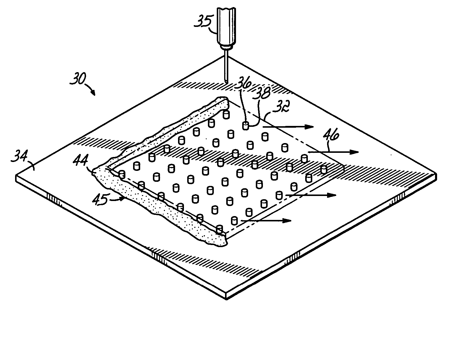
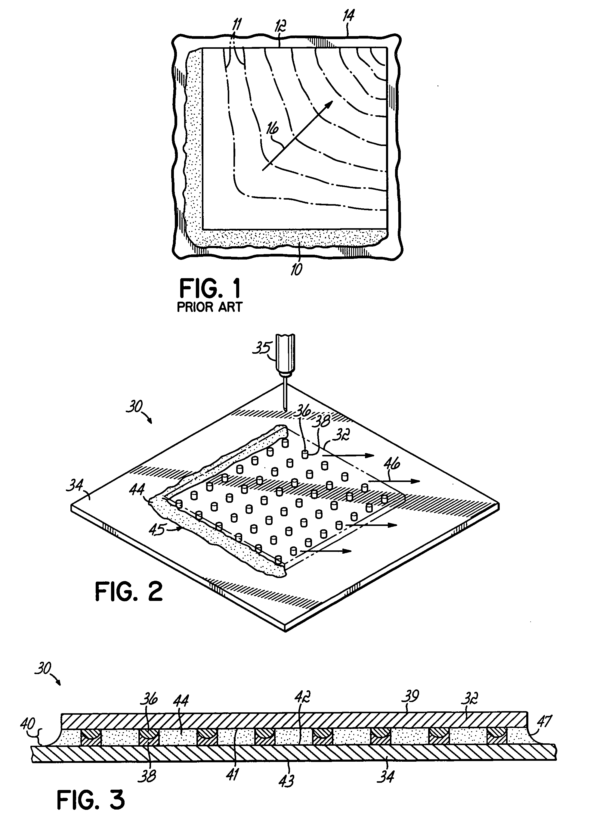
[0033] With reference to FIGS. 2 and 3, a semiconductor device package 30 consisting of a die 32 mounted on a package carrier or substrate 34 in a flip chip mounting arrangement is shown. As those skilled in the art will appreciate, substrate 34 may comprise an organic or ceramic substrate material such as a printed circuit board, a flip chip multi-chip module or a flip chip carrier. The die 32 is electrically and mechanically connected to the substrate 34 through an area array of solder bumps 36 on the underside of the die 32 that are registered or aligned with a corresponding area array of solder pads 38 on the substrate 34. Upon heating, the solder pads 38 on the substrate reflow and physically connect with the solder bumps 36 of die 32 to provide mechanical, thermal and electrical coupling therebetween in the form of solder joints. With this mounting arrangement, a gap 40 is formed between a contact side 41 of the die 32 and a top surface 42 of the substrate 34.

[0034] The gap 4...


PUM

PropertyMeasurementUnit
impingement angleaaaaaaaaaa
heat energyaaaaaaaaaa

Abstract

A method and apparatus for underfilling a gap between a multi-sided die and a substrate with an encapsulant material. The die and / or the substrate is heated non-uniformly by a heat source to generate a temperature gradient therein. The heated one of the die and the substrate transfers heat energy in proportion to the temperature gradient to the encapsulant material moving in the gap. The differential heat transfer steers, guides or otherwise directs the movement of the encapsulant material in the gap. The temperature gradient may be established with heat transferred from the heat source to the die and / or the substrate by conduction, convection, or radiation. The temperature gradient may be dynamically varied as the encapsulant material moves into the gap.

Description

CROSS-REFERENCE TO RELATED APPLICATIONS [0001] The present application is a continuation of application Ser. No. 10 / 408,464, filed Apr. 7, 2003, which claims the benefit of U.S. Provisional Application Ser. No. 60 / 371,826, filed Apr. 11, 2002, the disclosure of which is hereby incorporated herein by reference in its entirety.FIELD OF THE INVENTION [0002] This invention relates generally to liquid dispensing methods and apparatus used in semiconductor package manufacturing and, more particularly, to the underfilling of one or more semiconductor dies carried by a substrate. BACKGROUND OF THE INVENTION [0003] In the microelectronics industry, a die carrying an integrated circuit is commonly mounted on a package carrier, such as a substrate, a circuit board or a leadframe, that provides electrical connections from the die to the exterior of the package. In one such packaging arrangement called flip chip mounting, the die includes an area array of electrically-conductive contacts, known ...

Claims


Application Information

Patent Timeline
Patent Type & Authority Applications(United States)
IPC IPC(8): H01L21/56
CPCH01L21/563H01L2924/01065H01L2224/16H01L2224/73203H01L2224/83102H01L2224/92125H01L2924/0102H01L2924/01025H01L2924/01042H01L2924/01052H01L2924/01073H01L2924/01082H01L2924/14H01L2924/3011H01L2924/01006H01L2924/01033H01L2924/01043H01L24/28H01L2924/351H01L2924/15787H01L2924/12042H01L2924/00H01L21/56H01L21/50
Inventor QUINONES, HORATIOFANG, LIANGRATLEDGE, THOMAS LAFERL
Owner NORDSON CORP
Why Eureka
Try Eureka